A photodiode is a semiconductor device designed to convert light into electrical current. It operates under the principle of the photoelectric effect, where light photons are absorbed by the material, creating electron-hole pairs, and leading to current flow.
This article will explore the working, construction, types, applications, and other essential characteristics of photodiodes in a simple, easy-to-understand manner.
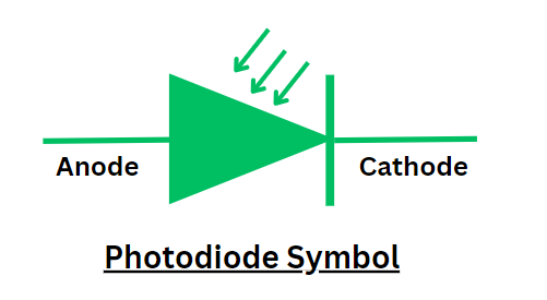
Symbol of a Photodiode
The symbol of a photodiode resembles that of a regular diode but with arrows pointing toward it, representing incoming light. The arrows indicate the light that falls on the device, leading to the current generation.
Construction of a Photodiode
The construction of a photodiode plays a critical role in its function of converting light into electrical signals. While the photodiode’s design is similar to a regular p-n junction diode, it is optimized to respond efficiently to incident light. The main components of a photodiode are its semiconductor material, optical window, and external terminals, each carefully designed for its specific role in light detection.
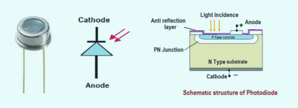
Semiconductor Material
The heart of a photodiode is its semiconductor material, typically silicon (Si) or germanium (Ge). These materials are selected for their ability to absorb light and generate electron-hole pairs, which are necessary for current generation. Depending on the application, other materials like gallium arsenide (GaAs) or indium gallium arsenide (InGaAs) may be used for photodiodes that need to detect specific wavelengths, such as infrared or ultraviolet light.
The semiconductor is typically in the form of a p-n junction, where p-type (positive) and n-type (negative) regions are formed by doping the semiconductor with specific impurities. The p-type region has an abundance of holes (positive charge carriers), while the n-type region has an excess of electrons (negative charge carriers). The interface between these regions forms the depletion region, where the photodiode’s core activity occurs.
Depletion Region
The depletion region is the most important part of the photodiode, where electron-hole pairs are generated when light photons hit the device. This region is devoid of free-charge carriers, creating a barrier where an electric field is established. When the photodiode is reverse-biased, this electric field strengthens, expanding the depletion region and making it more sensitive to light.
In some types of photodiodes, such as PIN photodiodes, an intrinsic (undoped) layer is inserted between the p-type and n-type regions, creating a larger depletion region. This construction enhances the sensitivity and performance of the photodiode, especially under low-light conditions.
Optical Window or Lens
One of the distinguishing features of a photodiode is its optical window or lens, which allows light to pass through and reach the semiconductor’s active area. The optical window is made of a transparent material, typically glass or plastic, designed to minimize reflection and absorb the maximum amount of light. In some photodiodes, an antireflective coating is applied to the window to further improve light transmission efficiency.
The window’s size and positioning are optimized to focus the incident light onto the depletion region for maximum light absorption. In some designs, a lens may be used to concentrate the incoming light onto a smaller, more sensitive area of the photodiode.
Metal Contacts and Package
For external electrical connections, metal contacts are attached to the p-type and n-type regions of the photodiode. These contacts are usually made from metals like aluminum, which offer good conductivity and minimal resistance. They allow the photodiode to be integrated into circuits by providing a pathway for the current generated by the movement of electron-hole pairs.
The entire photodiode assembly is housed in a protective package. This package is designed to protect the semiconductor material and internal components from environmental factors like dust, moisture, and mechanical stress while still allowing light to reach the depletion region. Photodiode packages come in various shapes and sizes, depending on their intended use. Some are small and flat for compact devices, while others may be cylindrical or rectangular, with an opening that directly faces the light source.
Working of a Photodiode
A photodiode operates on the principle of converting light into an electrical current, a phenomenon known as the photoelectric effect. The core mechanism behind the photodiode’s working lies in its semiconductor structure, which is typically a p-n junction diode. The device is engineered to operate in reverse bias mode, where the p-type material is connected to the negative terminal, and the n-type material is connected to the positive terminal of an external power supply.
When no light falls on the photodiode, it behaves like a regular diode, conducting a very small reverse current known as dark current. However, when light photons strike the depletion region of the diode, the magic begins. The energy from these photons is absorbed by the semiconductor material, which in turn excites electrons, knocking them out of their atomic bonds. This process generates electron-hole pairs within the depletion region.
The depletion region, which is essentially an area devoid of free charge carriers, plays a pivotal role in the photodiode’s working. The electrons are attracted towards the n-type region, while the holes drift towards the p-type region. This movement of charge carriers generates a current known as the photocurrent. The photocurrent is proportional to the intensity of the incident light, meaning that the stronger the light, the higher the number of electron-hole pairs generated, and consequently, the larger the current.
Since the photodiode is reverse-biased, the electric field across the depletion region is already strong. This field helps in swiftly sweeping the electrons towards the n-side and holes towards the p-side, ensuring a fast response to changing light levels. This ability to react quickly to light intensity variations makes photodiodes particularly useful in high-speed applications such as optical communication systems.
One critical feature of photodiodes is that they only respond to specific wavelengths of light. The wavelength sensitivity depends on the material used in constructing the diode, allowing photodiodes to be tailored for different applications, including visible, infrared, or ultraviolet light detection.
In summary, the working of a photodiode revolves around its ability to absorb photons, create electron-hole pairs, and generate a current proportional to the light intensity. Its efficient conversion of light into electrical signals, coupled with its fast response time, makes it a fundamental component in light-sensing technologies.
Types of Photodiodes
- PN Junction Photodiode: The most basic form, where the p-n junction is reverse biased, and the photocurrent depends on the light intensity.
- PIN Photodiode: It has an intrinsic (undoped) layer between the p-type and n-type regions, increasing the depletion region and making it more sensitive to low-light levels.
- Avalanche Photodiode: Operates at high reverse voltage and provides internal gain by using the avalanche effect to amplify the photocurrent.
- Schottky Photodiode: Has a metal-semiconductor junction, allowing for fast response time, commonly used in high-speed applications.
Modes of Operation
A photodiode is a semiconductor device used to convert light into electrical current. It operates under different modes, depending on the application and the type of light detection required. The primary modes of operation are Photovoltaic Mode, Photoconductive Mode, and Avalanche Mode. Each mode leverages the device’s inherent characteristics to serve specific functions in various light-sensing and detection applications.
1. Photovoltaic Mode
Photovoltaic mode, also known as zero-bias mode, is one of the fundamental operating modes of a photodiode. In this mode, the photodiode is not externally biased (no external voltage is applied). Instead, the device generates a voltage when it is exposed to light. This mode is based on the photovoltaic effect, which is the principle behind solar cells.
When photons of sufficient energy strike the depletion region of the p-n junction, they excite electrons, creating electron-hole pairs. The separation of these pairs due to the built-in electric field at the depletion region results in a current flow, which produces a measurable voltage across the diode’s terminals. The magnitude of the generated voltage is directly proportional to the intensity of the incident light.
Photodiodes in photovoltaic mode are widely used in low-speed applications like solar panels and light meters. The advantages of this mode include simplicity, as no external power supply is needed, and its energy-efficient nature. However, the disadvantages are its slow response time and relatively lower sensitivity compared to other modes.
2. Photoconductive Mode
Photoconductive mode is the most commonly used mode for photodiodes, particularly in high-speed applications like fiber-optic communication and optical sensors. In this mode, the photodiode is reverse biased, meaning a voltage is applied across the p-n junction in the reverse direction. The reverse bias significantly widens the depletion region, increasing the photodiode’s sensitivity to light.
When light photons hit the depletion region, electron-hole pairs are generated, just as in photovoltaic mode. However, the applied reverse bias enhances the electric field, causing the electron-hole pairs to separate faster and more efficiently. Electrons are drawn to the n-type side, and holes to the p-type side, leading to a rapid and strong photocurrent.
The primary advantage of photoconductive mode is its fast response time. The larger electric field created by the reverse bias enables the photodiode to quickly respond to changes in light intensity, making it ideal for high-speed data transmission and communication systems. Additionally, the reverse bias makes the device more sensitive to low light levels.
However, photoconductive mode has its disadvantages. The presence of dark current, a small current that flows even in the absence of light, can affect the accuracy of measurements in very low-light conditions. Also, the need for an external bias power supply adds complexity to the circuit.
3. Avalanche Mode
Avalanche mode is a specialized mode of operation used in avalanche photodiodes (APDs), where the photodiode is operated under a high reverse bias, often close to the breakdown voltage. This mode uses the principle of avalanche multiplication, where a single photon can cause the generation of multiple electron-hole pairs, effectively amplifying the photocurrent.
When a photon strikes the depletion region of an avalanche photodiode, it generates an electron-hole pair. Under the strong electric field of the reverse bias, the electrons and holes gain enough kinetic energy to knock out more electrons from their atomic bonds, causing an avalanche effect. This results in a significant amplification of the photocurrent, making avalanche photodiodes highly sensitive to low light levels.
Avalanche mode is particularly useful in applications that require high sensitivity, such as LIDAR (Light Detection and Ranging), medical imaging, and high-speed communication systems. The advantage of this mode is the internal gain that amplifies the signal without requiring external amplification circuits. This makes the APD more efficient in detecting faint light signals.
However, avalanche mode comes with disadvantages. Operating at high reverse bias voltages increases the risk of damage to the diode if not carefully controlled. Moreover, avalanche photodiodes tend to have higher noise levels, which can limit their performance in very precise applications.
Each mode of operation in a photodiode serves distinct purposes, tailored to different applications based on the requirements for speed, sensitivity, and signal strength. Photovoltaic mode is suitable for energy-efficient applications like solar panels, while photoconductive mode offers fast response times for high-speed communications. Avalanche mode provides extreme sensitivity but comes with complexities like higher noise and bias requirements. Understanding these modes helps in selecting the right type of photodiode for a specific application, ensuring optimal performance and efficiency.
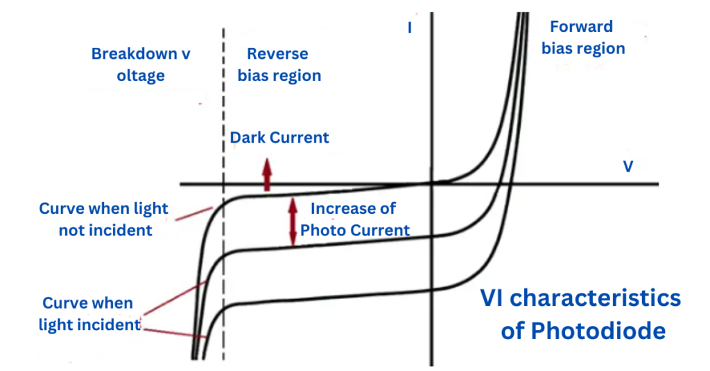
VI Characteristics of a Photodiode
The VI (Voltage-Current) characteristics of a photodiode provide valuable insights into how the device behaves under different conditions of light and biasing. A photodiode’s performance is influenced by the intensity of light, the applied voltage, and the inherent properties of its semiconductor material.
A photodiode typically operates in reverse bias mode, where a reverse voltage is applied across the p-n junction. The current through the photodiode, known as photocurrent, is a function of the incident light intensity. In the absence of light, a small reverse current known as dark current flows through the diode due to the thermal generation of charge carriers. When light falls on the depletion region, the photodiode generates electron-hole pairs, which lead to a noticeable increase in current. This current-voltage relationship defines the VI characteristics.
Dark Current (In Absence of Light)
In ideal conditions, when no light is present, a reverse-biased photodiode should have zero current. However, in practice, there is always a small leakage current, referred to as dark current. This current arises due to thermally generated electron-hole pairs in the semiconductor, even in the absence of photons. Dark current is undesirable as it adds noise to the system, reducing the photodiode’s sensitivity, particularly in low-light applications.
Dark current increases with the applied reverse voltage and is also temperature-dependent. At higher temperatures, the thermal generation of electron-hole pairs increases, leading to higher dark current. This characteristic makes it essential to consider temperature control in applications requiring high accuracy, such as in medical instruments or precision light meters.
Photocurrent (In Presence of Light)
When the photodiode is exposed to light, its behavior changes significantly. Light photons with energy greater than or equal to the semiconductor bandgap are absorbed in the depletion region, creating electron-hole pairs. These charge carriers are separated by the electric field in the depletion region, with electrons moving towards the n-side and holes towards the p-side, resulting in an increase in current. This is known as photocurrent.
The magnitude of the photocurrent is directly proportional to the intensity of the incident light. More photons result in the generation of more electron-hole pairs, which increases the photocurrent. This linear relationship between light intensity and photocurrent makes photodiodes highly suitable for applications like light intensity measurement, where precise detection of light is critical.
Reverse Bias Region
In reverse bias, the photodiode is connected such that the n-type material is connected to the positive terminal of the power supply, and the p-type material is connected to the negative terminal. This reverse biasing widens the depletion region, increasing the electric field across the junction. As a result, the photodiode becomes more sensitive to light, and the response time is reduced.
In the reverse bias region, the VI characteristics are influenced by two factors: the applied reverse voltage and the light intensity. As the reverse voltage increases, the photocurrent increases until it saturates. Beyond this point, further increases in reverse voltage have minimal effect on the photocurrent. The saturation region is where the photodiode operates efficiently, delivering a constant current for a given light intensity.
Forward Bias Region
Although photodiodes are usually operated in reverse bias, their VI characteristics in forward bias are similar to a regular p-n junction diode. In forward bias, the photodiode exhibits a significant increase in current with increasing forward voltage, but this mode is rarely used for light detection because the photocurrent is minimal and overshadowed by the forward conduction current.
Breakdown Region
At very high reverse voltages, the photodiode can enter the breakdown region. In this region, the reverse voltage is so high that it causes an avalanche effect, where the kinetic energy of charge carriers becomes sufficient to ionize atoms in the depletion region, generating additional electron-hole pairs. This results in a dramatic increase in current. While this effect is undesirable in standard photodiodes, it is intentionally exploited in avalanche photodiodes (APDs) to amplify weak optical signals.
Key Parameters Influencing VI Characteristics
Several factors affect the VI characteristics of a photodiode, including:
- Material Properties: The choice of semiconductor material (e.g., silicon, germanium) impacts the photodiode’s sensitivity to different wavelengths of light.
- Temperature: As temperature rises, dark current increases, which can affect the accuracy of light detection.
- Reverse Bias Voltage: Higher reverse bias widens the depletion region and enhances sensitivity, but excessive voltage can lead to breakdown.
- Light Intensity: The photocurrent increases proportionally to the light intensity, making this the most important factor in most applications.
The VI characteristics of a photodiode are crucial for understanding its behavior in light-sensitive applications. Operating primarily in reverse bias mode, the photodiode generates a current proportional to the incident light intensity, with factors such as dark current, reverse voltage, and temperature influencing its performance. Proper management of these characteristics ensures optimal use of photodiodes in industries ranging from telecommunications to medical devices.
In the absence of light, a photodiode behaves like a normal reverse-biased diode. However, when light hits the junction, the reverse current (known as photocurrent) increases with light intensity. The key aspects of VI characteristics include:
- Reverse bias: A small reverse current flows in the absence of light.
- Photocurrent: The current increases linearly with light intensity when the photodiode is illuminated.
- Dark current: This is the small current that flows even in the absence of light due to thermal generation of charge carriers.
Applications of Photodiodes
Photodiodes are widely used in applications where light detection or measurement is crucial. Common applications include:
- Optical Communication: To convert light signals into electrical signals in fiber optic networks.
- Light Meters: Used in cameras and environmental sensors to measure light intensity.
- Solar Cells: Large photodiodes are used in solar panels to convert light into electrical energy.
- Smoke Detectors: To detect smoke particles by measuring light absorption.
- Medical Devices: Used in pulse oximeters and medical imaging devices to monitor light absorption.
Advantages of Photodiodes
- Fast response time: Can detect rapid changes in light intensity.
- High sensitivity: Especially in PIN and avalanche photodiodes.
- Compact size: Small and easy to integrate into electronic circuits.
- Low cost: Economical compared to other light detection devices.
- Wide spectral response: Capable of detecting light across different wavelengths.
Disadvantages of Photodiodes
- Requires external bias: Often needs reverse biasing, which adds complexity to circuits.
- Temperature sensitivity: Performance can degrade with temperature fluctuations.
- Dark current: This noise current can affect the accuracy of light detection in very low-light conditions.
- Limited light-to-current efficiency: Not all absorbed light is converted into current, leading to energy losses.
Characteristics of Photodiodes
- Responsivity: The efficiency with which the photodiode converts light into electrical current, measured in Amps per Watt.
- Quantum Efficiency: The ratio of the number of charge carriers generated to the number of incident photons.
- Dark Current: The small current that flows in the absence of light due to thermal activity.
- Response Time: The time taken by the photodiode to respond to changes in light intensity, which is critical in high-speed applications.
- Noise Equivalent Power (NEP): The minimum amount of light power the photodiode can detect over a given bandwidth, considering noise.
Conclusion
The photodiode is a versatile component used in various applications, from communication systems to everyday devices like cameras. Its ability to quickly convert light into electrical signals, combined with its compact size, makes it an essential part of modern electronics. Understanding its construction, working principles, and characteristics allows for more effective use in both simple and complex electronic systems.