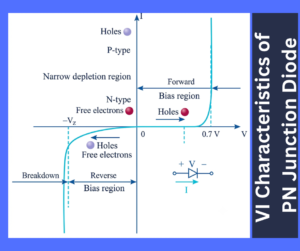
VI Characteristics of a PN Junction Diode
The VI characteristics of a PN junction diode describe the relationship between the voltage applied across the diode and the current flowing through it under
The VI characteristics of a PN junction diode describe the relationship between the voltage applied across the diode and the current flowing through it under
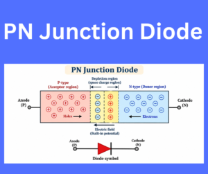
A PN-junction diode is created by joining p-type and n-type semiconductor materials. This junction develops a built-in potential barrier that regulates the movement of charge
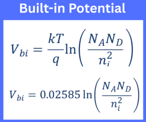
The built-in potential is an important concept in semiconductor physics, particularly in understanding the operation of a PN junction diode. It is the internal voltage
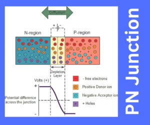
A PN junction is formed by joining P-type and N-type semiconductor regions within a single semiconductor crystal. The junction creates the basic structure of a
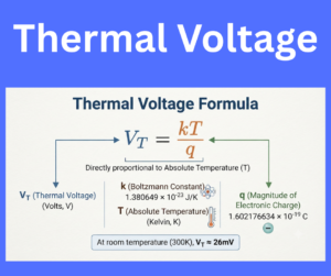
Thermal voltage is an important parameter in semiconductor physics that represents the ratio of thermal energy to the electric charge of a carrier. It is
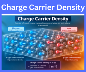
Charge carrier density is a key parameter in semiconductor physics and electronic device design. It helps engineers understand how materials respond to electrical and thermal
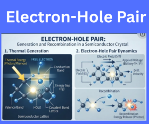
Electron-hole pair are fundamental to understanding how semiconductor materials respond to external energy. Their formation and behavior influence the availability of charge carriers, while their

Charge carriers play a vital role in determining the electrical properties of materials. Their behavior varies with the material structure, temperature, and presence of impurities.

Reverse leakage current is an important parameter used to evaluate the performance of semiconductor diodes. It indicates how much unwanted current passes through a diode
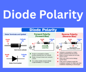
Diode polarity refers to the orientation of a diode in an electrical circuit and determines whether the device is forward-biased or reverse-biased. A diode has