A clamper circuit is a fundamental electronic circuit used to shift the voltage level of a signal without distorting its waveform. These circuits play a crucial role in signal processing, voltage regulation, and waveform stabilization, ensuring precise control over signal positioning. A clamper circuit modifies signal reference points by adding a DC level to an AC signal, making it indispensable in various applications such as television receivers, oscilloscopes, and communication systems.
What is a Clamper Circuit?
A clamper circuit, also known as a clamping circuit, is an electronic circuit that adds a DC level to an AC signal without altering its waveform. These circuits are essential in electronic applications as they enable voltage level modifications while preserving signal integrity. By shifting the DC level, a clamper circuit is also referred to as a Level Shifter.
A clamper circuit consists of energy storage elements like capacitors, along with a diode, a resistor, and, if required, a DC battery. The positive and negative peaks of a signal can be placed at desired levels using clamper circuits, making them useful in voltage regulation and signal processing. Clamper circuits use a combination of diodes, capacitors, DC restorers, or clamped capacitors to achieve the desired voltage shift.
To maintain the time period of the waveform, the time constant (τ)=RC must be greater than half the time period. C and R are the capacitance and resistance in the circuit. This ensures that the discharging time of the capacitor is slow and does not distort the waveform.
The DC component present in the input is rejected when a capacitor-coupled network is used, as capacitors block DC. Therefore, when DC needs to be restored, a clamping circuit is used.
Types of Clampers
Clamper circuits can be categorized into the following types:
- Positive Clamper
- Positive Clamper with Positive Reference Voltage (Vr)
- Positive Clamper with Negative Reference Voltage (Vr)
- Negative Clamper
- Negative Clamper with Positive Reference Voltage (Vr)
- Negative Clamper with Negative Reference Voltage (Vr)
Let’s explore each type in detail.
Positive Clamper Circuit
A positive clamper circuit consists of a diode, a resistor, and a capacitor, which shift the output signal towards the positive portion of the input signal.
A clamping circuit restores the DC level of a signal. When the negative peak of the signal is raised above zero, the signal is said to be positively clamped.
The construction and working of a positive clamper circuit are explained below.

- Initially, when the input is applied, the capacitor is uncharged, and the diode is reverse-biased. The output is not considered at this point.
- During the negative half cycle, at the peak value, the capacitor charges with a negative voltage on one plate and a positive voltage on the other. At this moment, the diode is forward-biased and conducts heavily.
- During the positive half cycle, the capacitor is charged to Vm (peak voltage) while the diode becomes reverse-biased and is open-circuited. The output of the circuit at this stage is: Vo= Vi+Vm
- Hence, the signal is positively clamped, shifting the entire waveform in the positive direction. The output signal follows the input signal but remains shifted upwards due to the charge stored in the capacitor.
Positive Clamper with Positive Vr
A positive clamper circuit, when biased with a positive reference voltage, results in the addition of this voltage to the output signal, thereby elevating the clamped level. This allows precise control over the signal shift, making it particularly useful in waveform shaping and signal processing applications. The circuit diagram for a positive clamper with a positive reference voltage is shown below.
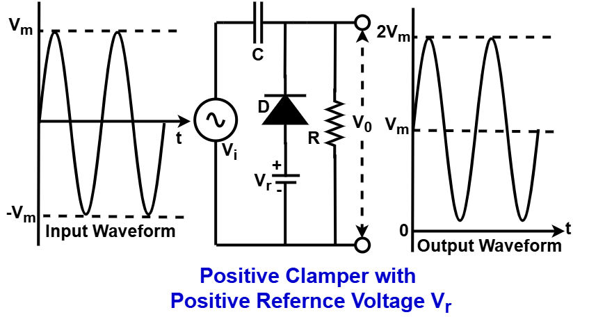
During the positive half-cycle of the input signal, the reference voltage is applied through the diode at the output. As the input voltage rises, the cathode voltage of the diode increases relative to the anode voltage. This causes the diode to become reverse-biased, preventing conduction.
During the negative half-cycle, the diode becomes forward-biased and starts conducting. This allows the capacitor to charge to the peak voltage of the input signal combined with the reference voltage. As a result, the output waveform is shifted upward, maintaining a consistent voltage level dictated by the sum of the capacitor voltage and the reference voltage.
This configuration ensures that the output waveform is positively clamped, preventing excessive negative excursions and stabilizing the signal for further processing in electronic applications.
Positive Clamper with Negative Vr
A positive clamper circuit, when biased with a negative reference voltage, shifts the output signal upwards by adding the reference voltage to it. This results in raising the clamped level of the waveform. The circuit diagram for a positive clamper with a negative reference voltage is illustrated below.
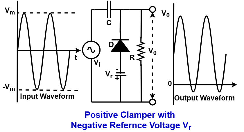
- During the positive half-cycle of the input signal, the voltage across the capacitor, along with the negative reference voltage, maintains the output voltage level. The diode remains reverse-biased and does not conduct during this phase.
- During the negative half-cycle, the input voltage decreases, and when the cathode voltage of the diode becomes lower than the anode voltage, the diode starts conducting. This allows the capacitor to charge and store energy.
- As a result, the output voltage is shifted upwards by the value of the reference voltage, ensuring a stable signal level without altering the waveform shape.
This type of clamper circuit is useful in applications where a controlled shift in signal level is required for processing or display purposes.
Negative Clamper
A negative clamper circuit is an electronic circuit that shifts the entire waveform of an AC signal downward, moving it toward the negative portion of the input signal. This type of clamping circuit consists of a diode, a resistor, and a capacitor, which work together to modify the signal’s DC level without changing its waveform. The construction and working of a negative clamper circuit are explained below.
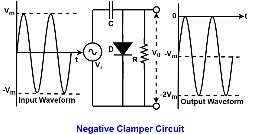
- Positive Half Cycle: During the positive half cycle of the input signal, the diode is forward-biased and conducts. This allows the capacitor to charge to its peak voltage (Vm) with the correct polarity. The capacitor stores this charge for the next cycle.
- Negative Half Cycle: When the input signal enters its negative half cycle, the diode becomes reverse-biased and stops conducting. The charged capacitor then shifts the signal downward by the peak voltage value (Vm), causing the output waveform to be negatively clamped.
- Output Voltage Equation: At this stage, the output voltage (V₀) is given by: V₀ = Vᵢ + Vₘ . This means the output signal maintains the same waveform as the input but with a shifted DC level.
Key Features of Negative Clamper Circuit
- The capacitor stores the charge and helps shift the signal downward.
- The diode controls when the circuit conducts and clamps the signal.
- The circuit does not distort the waveform, only modifies its DC level.
- Used in applications like TV signal processing, voltage regulation, and waveform shaping.
A negative clamper circuit is essential in various electronic applications where shifting a signal’s DC reference is required without altering its shape.
Negative clamper with positive Vr
A negative clamper circuit, when biased with a positive reference voltage, shifts the output signal downward while adding the reference voltage to the output. This helps in modifying the signal level without altering its waveform. The circuit diagram and its working for a negative clamper with a positive reference voltage are shown below.
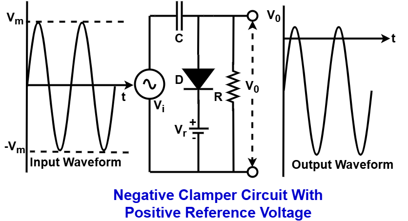
- Positive Half-Cycle: During the positive half-cycle of the input signal, the diode is forward-biased and conducts. At this stage, the output voltage is equal to the applied positive reference voltage.
- Negative Half-Cycle: When the input voltage enters the negative half-cycle, the diode becomes reverse-biased and stops conducting. The capacitor, which was charged during the positive half-cycle, now contributes to the output voltage.
- Output Voltage Behavior: Although the signal is negatively clamped, a portion of the waveform is raised to a positive level due to the applied reference voltage. This results in a controlled DC level shift.
Key Features
- The circuit shifts the signal downward while incorporating the reference voltage.
- The waveform remains unchanged, only its voltage level is adjusted.
- The capacitor and diode work together to control the clamping action.
- Used in applications like signal processing, waveform shaping, and voltage control.
This type of clamping circuit is useful in cases where a specific voltage shift is needed without distorting the original signal.
Negative Clamper with Negative Vr
A negative clamper circuit, when biased with a negative reference voltage, shifts the output signal downward while adding the reference voltage to the output. This allows precise control over the waveform’s DC level without altering its shape. The circuit diagram for a negative clamper with a negative reference voltage is shown below.
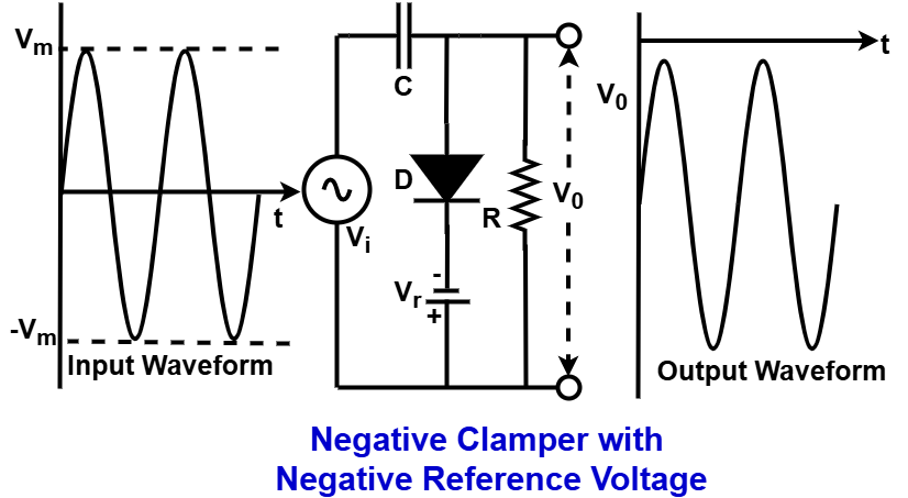
- Positive Half-Cycle: During the positive half-cycle of the input signal, the diode is forward-biased and starts conducting even before the zero voltage level is reached due to the applied negative reference voltage. This ensures that the capacitor charges accordingly.
- Negative Half-Cycle: When the input signal enters the negative half-cycle, the diode becomes reverse-biased and stops conducting. At this stage, the voltage across the capacitor appears at the output, shifting the waveform further downward.
- Output Voltage Behavior: As a result, the entire waveform is clamped further toward the negative side, effectively lowering the output signal’s voltage range.
Key Features
- The signal is shifted further downward due to the applied negative reference voltage.
- The waveform shape remains unchanged, while only its voltage level is adjusted.
- The diode and capacitor work together to control the clamping action.
- Used in applications such as signal processing, waveform shaping, and voltage control where a further negative shift is required.
This type of clamping circuit is useful when specific negative voltage level adjustments are needed without distorting the original signal.
Applications of Clampers
Clampers are widely used in electronic circuits for various applications. Some of the key applications include:
- Restoring DC Levels: Clamper circuits are used to restore the DC component of a signal that has been lost due to capacitor coupling.
- Signal Processing: Used in communication systems to shift signal levels without altering their waveform, ensuring proper data transmission.
- TV and Radar Systems: Employed in television receivers and radar systems to fix the signal waveform at a desired DC level.
- Oscilloscope Calibration: Used in oscilloscopes to adjust signal levels for accurate waveform display and analysis.
- Voltage Multipliers: Clampers play a crucial role in voltage multiplier circuits to increase the output voltage levels efficiently.
- Image Processing: Utilized in image sensors and processing circuits to maintain the brightness and contrast levels of images.
- Noise Reduction in Communication Circuits: Helps in reducing noise and unwanted distortions in analog and digital communication circuits.
- Protecting Electronic Components: Used in circuits to prevent unwanted voltage fluctuations that could damage sensitive components.
Benefits of Clampers
Clampers offer several advantages in electronic circuits. Some of the key benefits include:
- DC Level Shifting: Clampers adjust the DC level of signals without distorting their waveform, making them useful in signal processing applications.
- Waveform Preservation: Unlike amplifiers or other circuits, clampers maintain the original shape of the signal while shifting its voltage level.
- Enhanced Signal Transmission: In communication systems, clampers help in proper signal transmission by ensuring that voltage levels remain within the required range.
- Protection of Electronic Components: Clampers prevent voltage fluctuations that can damage sensitive electronic components, ensuring circuit stability and longevity.
These benefits make clamper circuits essential in various applications, including communication, signal conditioning, and electronic circuit protection.
Drawbacks of Clampers
Despite their advantages, clampers also have some limitations. Here are four key drawbacks:
- Limited Voltage Regulation: Clampers cannot provide precise voltage regulation as they only shift the DC level of a signal.
- Dependence on Circuit Components: The performance of a clamper circuit depends on the values of the diode, capacitor, and resistor, which can introduce variations in output.
- Not Suitable for High-Frequency Applications: At high frequencies, the capacitor may not charge and discharge effectively, affecting the circuit’s performance.
- Power Losses: Some power is lost due to the forward voltage drop across the diode, which can impact efficiency in low-voltage applications.
While clampers are useful in many applications, these limitations should be considered when designing circuits that require precise voltage control and high-frequency performance.
Conclusion
Clampers are essential electronic circuits used for shifting the DC level of signals without altering their waveform. They play a significant role in applications such as signal processing, voltage regulation, and waveform stabilization. By using diodes, capacitors, and resistors, clamper circuits effectively adjust voltage levels, making them valuable in various electronic and communication systems.
Despite their advantages, clampers have some limitations, such as dependency on circuit components, inefficiency in high-frequency applications, and minor power losses. However, their ability to preserve signal integrity while modifying voltage levels makes them indispensable in many practical applications.
Understanding the working principles, types, benefits, and drawbacks of clampers helps in designing efficient circuits for different electrical and electronic applications.
Read Next: