The inverting operational amplifier is one of the simplest and most widely used op-amp configurations. It produces an output voltage that is opposite in polarity and phase to the input voltage, while the amount of amplification is determined by the feedback and input resistor values.
Introduction to the Inverting Operational Amplifier
An Inverting Operational Amplifier is a common voltage amplifier configuration that increases the magnitude of an input signal while reversing its polarity. The input signal is applied to the inverting (−) terminal, and negative feedback is used to control the amplifier’s closed-loop gain.
As a result, a positive input voltage produces a negative output voltage, while a negative input produces a positive output. Thus, the output signal is 180° out of phase with the input, which is the characteristic feature of an inverting operational amplifier.
Controlling the Voltage Gain
As discussed in the previous operational amplifier basics tutorial, the open-loop gain of an operational amplifier can be extremely high, reaching 1,000,000 (120 dB) or more.
However, such a high gain is generally impractical for controlled amplification. Even a very small input signal of only a few microvolts (μV) can drive the output voltage toward one of the power-supply rails, causing saturation and making it difficult to maintain a predictable output.
Since the open-loop DC gain is so high, some of this gain can be intentionally sacrificed by connecting a suitable resistive or impedance feedback network from the output terminal back to the inverting input terminal.
This feedback network reduces and controls the effective gain of the amplifier. The process is known as negative feedback and provides a more stable and predictable operational amplifier circuit, with the closed-loop gain determined mainly by the external feedback components.
Using Negative Feedback
Negative feedback is the process of returning a portion of the output signal to the input in such a way that it opposes the original input. In an inverting op-amp circuit, the feedback is applied to the inverting (−) input, while the non-inverting (+) input is connected to ground or a zero-voltage reference.
An external feedback resistor, , connects the output to the inverting input. This feedback arrangement drives the differential input voltage toward zero under normal linear operation. The amplifier therefore operates as a closed-loop circuit, and its gain is referred to as the closed-loop gain.
Negative feedback reduces the very high open-loop gain but provides much better control and stability. The closed-loop gain can therefore be set accurately using the external feedback components.
Because the inverting input receives both the actual input signal and the feedback signal, it acts as a summing point. An input resistor, , is used to apply the input signal to this node while keeping it separate from the feedback path.
Since the non-inverting input is connected to ground, negative feedback causes the voltage at the inverting input to approach the same potential as the non-inverting input. For an ideal op-amp, this means:
The inverting input is therefore said to be at a virtual earth (virtual ground). It is not physically connected to ground, but it remains approximately at ground potential because of the op-amp’s negative-feedback action. This behavior is fundamental to the operation of the inverting operational amplifier.
Inverting Operational Amplifier Configuration
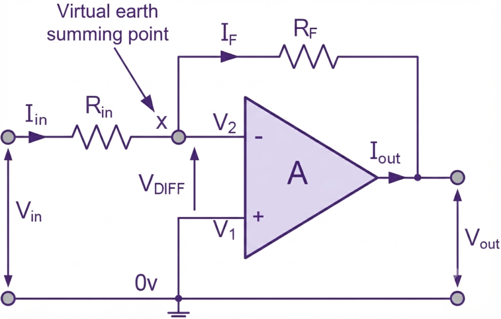
The input resistor connects the input voltage to the inverting (−) input, while the feedback resistor connects the output voltage back to the same inverting input. This feedback arrangement provides negative feedback, allowing the operational amplifier to operate as a stable closed-loop inverting amplifier.
For an ideal op-amp, two important assumptions are used when analysing an inverting amplifier: “no current flows into either input terminal” and “ is equal to ”. In practical op-amps, these conditions are approximations because small input currents and differential voltages can exist.
The junction X, where the input and feedback paths meet, remains at nearly the same voltage as the non-inverting (+) terminal. Since the non-inverting input is grounded, negative feedback keeps the inverting input close to 0 V, creating a virtual-earth condition.
Because of this virtual-earth node, the input resistance seen by the source is approximately equal to . The closed-loop gain can therefore be controlled by selecting the ratio of the two external resistors.
The two key rules for an inverting amplifier are:
- No current flows into the input terminals.
- The differential input voltage is approximately zero, so , producing the virtual-earth condition.
Using these assumptions, we can derive the closed-loop gain of the inverting amplifier from first principles.
Inverting Op-amp Configuration Mathematical Derivation for Voltage Gain
The input current flows through the series combination of resistors and , as shown below.
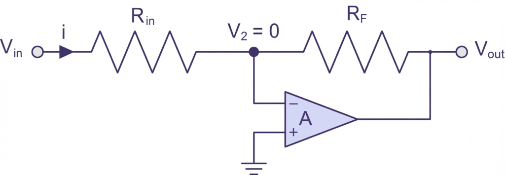
Therefore,
so,
and as,
Closed loop gain ( Av ) is given as,
Inverting Op-amp Voltage Gain Equation
Therefore, the closed-loop voltage gain formula of the inverting amplifier can be expressed as:
This expression can be rearranged to obtain the output voltage as:
The negative sign in the equation indicates that the output signal is inverted relative to the input signal, giving a 180° phase difference. This phase reversal is a characteristic of the inverting amplifier configuration and results from the way negative feedback is applied.
The output voltage equation also shows that, for a fixed closed-loop gain, the circuit has a linear relationship between input and output:
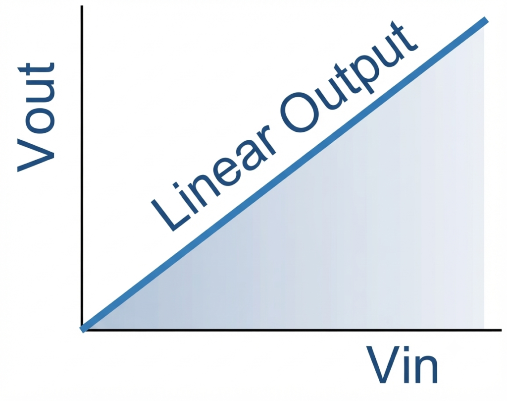
This linear amplification is particularly useful for increasing a low-level sensor signal to a higher voltage that can be more easily processed, measured, or monitored by other electronic circuits.
Inverting Operational Amplifier Worked Example No1
Find the closed-loop voltage gain of the following inverting operational amplifier circuit.
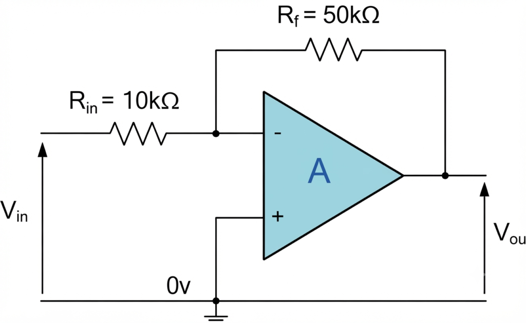
Using the formula for the closed-loop gain of an inverting operational amplifier:
We can substitute the given resistor values:
and,
Therefore, the gain of the circuit is calculated as:
The corresponding gain in decibels is:
Therefore, the closed-loop gain of the inverting amplifier is −5, or approximately 14 dB.
Inverting Op-amp Worked Example No2
The gain of the original circuit is to be increased to 20 (26.02 dB). Find suitable new resistor values.
For an inverting operational amplifier, the closed-loop voltage gain is:
Taking the input resistor as:
The required feedback resistor is:
Therefore, suitable resistor values are:
The resulting closed-loop gain is:
The gain magnitude in decibels is:
Therefore, the new resistor values are , giving a voltage gain of
Difference Between Inverting and Non-Inverting Op-Amp
The inverting and non-inverting operational amplifier configurations differ mainly in how the input signal is connected, the resulting voltage gain, and the phase relationship between input and output.
| Parameter | Inverting Op-Amp | Non-Inverting Op-Amp |
| Voltage Gain | AV = -Rf/RIN | AV = 1 + Rf/RIN |
| Phase Shift | Output is 180° out of phase with the input signal. | Output is in phase with the input signal. |
| Gain Range | Gain magnitude can be less than, equal to, or greater than 1. | Gain is always greater than or equal to 1. |
| Input Connection | Input is applied to the inverting (−) terminal through RIN. | Input is applied directly to the non-inverting (+) terminal. |
| Feedback | Negative feedback is applied to the inverting terminal through Rf. | Negative feedback is applied to the inverting terminal through the resistor network. |
| Input Impedance | Approximately equal to the input resistor RIN. | Very high, determined mainly by the op-amp input impedance. |
| Output Polarity | Output polarity is opposite to the input. | Output polarity follows the input. |
Note: The “output high for ” and “output high for ” statements in the original table describe a comparator, not ordinary inverting/non-inverting amplifiers, so they should not be included in this comparison.
Advantages of Inverting Operational Amplifier
The inverting operational amplifier offers several practical advantages that make it useful in analog circuit design:
- Stable and predictable gain: Negative feedback provides a well-controlled closed-loop gain, making the circuit easier to analyze and design.
- Adjustable voltage gain: The gain depends mainly on the ratio of the feedback and input resistors. By selecting suitable resistor values, both low and high levels of voltage amplification can be achieved.
- Virtual ground: With the non-inverting input connected to ground, the inverting input remains approximately at 0 V under negative feedback. This virtual ground simplifies circuit analysis and design.
- Phase inversion: The output signal is 180° out of phase with the input. This phase-inverting property is useful in signal-processing and phase-related circuits.
- High input and low output impedance: The op-amp itself provides very high input impedance and low output impedance. This minimizes loading of the source and allows the amplifier to drive relatively low-impedance loads more effectively.
- Simple circuit configuration: The basic circuit requires only an op-amp and two resistors to establish the closed-loop gain, making it straightforward to implement.
Disadvantages of Inverting Operational Amplifier
Although an inverting operational amplifier offers simple gain control and phase inversion, it also has some limitations that should be considered during circuit design:
- Input impedance depends on the input resistor: The source sees approximately as the input impedance. A low resistor value can therefore increase the current drawn from the source and cause loading.
- Input noise contribution: The input resistor and feedback network contribute thermal and other noise sources. This can be important in low-level signal and precision applications.
- Limited gain and bandwidth: Increasing the closed-loop gain reduces the available bandwidth because practical op-amps have a finite gain-bandwidth product. The output is also limited by the op-amp’s supply voltage and output-drive capability.
- Offset and bias-current errors: Practical op-amps have input offset voltage and input bias currents. These non-ideal characteristics can introduce errors at the output, particularly when high resistor values are used.
- Phase inversion may be undesirable: The output is 180° out of phase with the input. If an application requires an in-phase output, an additional non-inverting stage or another circuit configuration may be needed.
- Resistor values affect performance: Very large or very small resistor values can introduce practical problems such as increased noise, input bias-current errors, or excessive loading. Suitable resistor values should therefore be selected according to the op-amp and application.
Applications of Inverting Operational Amplifier
The inverting operational amplifier is widely used in analog electronics because its gain, phase response, and signal-processing characteristics can be controlled using external components. Common applications include:
- Phase-shift circuits: The configuration introduces a 180° phase reversal between the input and output, making it useful in circuits where signal polarity or phase must be reversed.
- Oscillator circuits: Inverting op-amp stages can be incorporated into oscillator designs to provide the required gain and phase relationships for generating periodic waveforms.
- Integrator and differentiator circuits: By replacing or combining feedback resistors and capacitors, the inverting configuration can perform integration and differentiation of input signals. These circuits are widely used in analog signal processing.
- Signal amplification: The most common application is the inverting amplifier, where an input voltage is amplified and inverted. The voltage gain is determined by the ratio of the feedback resistor to the input resistor.
- Schmitt trigger and signal conditioning: Op-amp circuits with positive feedback can be configured as Schmitt triggers to convert noisy or slowly varying signals into clean switching waveforms with defined threshold levels.
Conclusion
The Inverting Operational Amplifier is one of the two fundamental op-amp configurations, along with the non-inverting operational amplifier. It amplifies the input signal while reversing its phase by 180°. As a result, a positive input produces a negative output, and a negative input produces a positive output.
The very high open-loop gain of an op-amp can be controlled using two external resistors. The input resistor connects the input signal to the inverting terminal, while the feedback resistor connects the output back to the same terminal. The non-inverting input is normally connected to ground (0 V).
The closed-loop voltage gain is determined by the ratio of the feedback resistance to the input resistance:
The negative sign indicates the 180° phase inversion between the input and output signals.
When the two resistors have equal values, , the voltage gain becomes −1:
This configuration is known as a unity-gain inverter or inverting buffer because it maintains the input voltage magnitude while reversing its polarity.
In the next tutorial, we will examine the complementary Non-Inverting Operational Amplifier, where the output remains in phase with the input signal.
Read Next: