Discover the key difference between PN junction diode and Zener diode, including their working principles, applications, doping levels, and conduction properties. Learn how PN junction diodes are used for rectification, while Zener diodes play a crucial role in voltage regulation and overvoltage protection.
Both PN junction diodes and Zener diodes are essential semiconductor devices widely used in electronic circuits. A PN junction diode primarily serves as a rectifier, converting AC to DC, whereas a Zener diode is designed for voltage regulation, maintaining a stable voltage level.
There are several key differences between these two diodes, which are detailed in the table below. Before exploring these differences, it is beneficial to understand the fundamental concepts of both PN junction diodes and Zener diodes.
The PN junction diode operates in forward bias to allow current flow and in reverse bias to block it, making it ideal for rectification applications in power supplies. It is commonly found in circuits requiring unidirectional current flow, such as AC-to-DC converters and signal demodulation circuits.
On the other hand, a Zener diode is specifically designed to operate in reverse bias beyond its breakdown voltage without damage. This unique property makes it an excellent choice for voltage regulation and overvoltage protection in power supplies and electronic circuits. Unlike a standard diode, the Zener diode maintains a constant output voltage, ensuring the stability of sensitive components.
Before delving into the differences between a PN junction diode and a Zener diode, it is essential to first understand their fundamental characteristics and working principles
What is a PN Junction Diode?
A PN junction diode is a two-terminal semiconductor device formed by joining a p-type semiconductor with an n-type semiconductor, creating a PN junction. This junction is the key feature that allows the diode to control current flow. The two terminals of the diode are called the anode (positive) and cathode (negative).
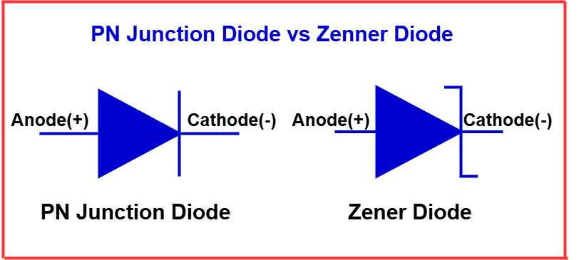
When a voltage is applied, current flows from the anode to the cathode, allowing the diode to function as a unidirectional device. The standard circuit symbol for a PN junction diode is depicted in the figure below.

The PN junction diode is widely used in various electronic applications due to its ability to control current flow effectively.
The PN junction diode conducts only in the forward bias condition, meaning it allows current to flow when the anode is connected to the positive terminal of a power source and the cathode is connected to the negative terminal. In reverse bias, the diode acts as an open switch and does not conduct.
Due to this property, PN junction diodes are widely used in rectification applications, where they convert AC (alternating current) into DC (direct current). Additionally, they play a crucial role in signal processing, voltage clamping, and protection circuits, making them essential components in power supplies and various electronic devices.
What is a Zener Diode?
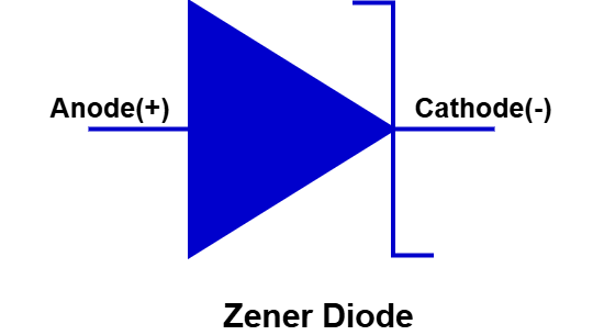
A Zener diode is a specially designed semiconductor diode that operates in the breakdown region without damage. Like a standard PN junction diode, it has two terminals: anode and cathode. However, the key difference is that the Zener diode is engineered to function reliably even when subjected to reverse bias breakdown conditions. The standard circuit symbol for a zener diode is depicted in the figure below.
The Zener diode is made by joining a highly doped p-type semiconductor with a highly doped n-type semiconductor. Due to this high doping level, it has a greater concentration of charge carriers (electrons and holes) than a standard PN junction diode. This unique property allows it to maintain a stable voltage under varying current conditions.
In forward bias, a Zener diode behaves like a regular PN junction diode, allowing current to flow. However, in reverse bias, when the applied voltage reaches the Zener voltage, the depletion layer undergoes a controlled breakdown known as Zener breakdown, enabling current conduction in the reverse direction.
This ability to conduct in both forward and reverse directions makes the Zener diode highly effective as a voltage regulator. It is widely used in power supply circuits, overvoltage protection, and voltage reference applications, ensuring that sensitive components receive a constant and stable voltage.
One of the key characteristics of a Zener diode is its Zener voltage, which determines the voltage at which it starts conducting in reverse bias. Zener diodes are available in different voltage ratings, typically ranging from a few volts to several hundred volts, making them versatile for various electronic applications.
Additionally, the power dissipation capacity of a Zener diode plays a crucial role in its performance. It is essential to select a Zener diode with an appropriate power rating to prevent overheating and ensure reliable operation under different load conditions. Heat sinks or series resistors are often used to control power dissipation.
Due to their high stability and precision, Zener diodes are commonly found in voltage reference circuits, clamping circuits, and waveform-shaping applications. Their ability to regulate voltage makes them an integral part of modern electronic systems, ensuring efficiency and protection against voltage fluctuations.
Difference between PN Junction Diode and Zener Diode
The PN junction diode and Zener diode are both semiconductor devices used in electronic circuits. However, they have distinct properties and applications. The table below highlights the key differences between the two:
| Parameter | PN Junction Diode | Zener Diode |
|---|---|---|
| Definition | A two-terminal semiconductor device formed by joining a p-type and an n-type semiconductor. It allows current flow in one direction only. | A special type of semiconductor diode designed to operate in the breakdown region for voltage regulation. |
| Doping level | Low doping of p-type and n-type semiconductors. | Highly doped p-type and n-type semiconductors. |
| Width of depletion layer | Wider depletion layer due to low doping. | Narrow depletion layer due to high doping. |
| Effect of reverse current | High reverse current can damage the diode. | Can sustain high reverse current without damage. |
| Breakdown voltage | High breakdown voltage. | Lower breakdown voltage, designed to operate in breakdown mode. |
| Biasing condition | Works in forward bias, blocking current in reverse bias. | Works in reverse bias beyond the breakdown voltage. |
| Ohm’s Law | Obeys Ohm’s Law in the forward direction. | Does not obey Ohm’s Law in the reverse breakdown region. |
| Manufacturing materials | Made from silicon or germanium, with silicon being more common. | Material depends on required breakdown voltage. |
| Current flow | Allows current flow in one direction (forward bias). | Allows current flow in both forward and reverse bias (above breakdown voltage). |
| Behavior in forward & reverse bias | Acts as a closed switch in forward bias and an open switch in reverse bias. | Acts as a normal diode in forward bias and conducts in reverse bias beyond breakdown voltage. |
| Application | Used in rectification, clipping, clamping, and signal demodulation. | Mainly used as a voltage regulator and overvoltage protection. |
| Power dissipation | Designed for low power dissipation. | Capable of handling high power dissipation in reverse breakdown mode. |
| Voltage stability | Does not regulate voltage. | Maintains a stable output voltage under varying input conditions. |
| Response to temperature changes | Performance varies significantly with temperature. | Designed for better temperature stability, making it suitable for voltage reference circuits. |
| Symbol Representation | Represented with a simple diode symbol. | Represented with a diode symbol with bent ends indicating reverse breakdown behavior. |
| Usage in circuits | Found in AC-to-DC converters, amplifiers, and logic circuits. | Used in power supplies, surge protection circuits, and precise voltage references. |
Both diodes play crucial roles in electronics, with PN junction diodes primarily used for rectification, while Zener diodes ensure voltage regulation and circuit protection.
Conclusion
In summary, the key distinction between a PN junction diode and a Zener diode lies in their conduction properties. A PN junction diode permits current flow only in the forward direction, whereas a Zener diode allows current to flow in both forward and reverse directions when operating in its breakdown region.
Due to these characteristics, PN junction diodes are primarily used for rectification, converting AC to DC, while Zener diodes are widely used for voltage regulation and overvoltage protection in electronic circuits. Understanding these differences helps in selecting the right diode for specific applications.
Read Next: