Discover the key differences between NPN and PNP transistor, including their structure, working principles, charge carriers, current flow, and applications. Learn how to choose the right transistor for switching and amplification in electronic circuits.
A transistor, also known as a bipolar junction transistor (BJT), is a three-terminal, three-layer, and two-junction semiconductor device used as a digital switch and amplifier in electronic circuits. It consists of three layers made from P-type and N-type semiconductor materials, named the emitter, base, and collector, with terminals drawn from each layer.
A transistor operates by controlling the flow of current between the collector and emitter terminals, with the base terminal acting as a control gate. A small current applied to the base can regulate a much larger current flowing through the collector-emitter path, making transistors essential components in signal amplification and switching applications.
Transistors are classified into two types based on the arrangement of the semiconductor layers:
- NPN Transistor
- PNP Transistor
The primary difference between NPN and PNP transistors lies in the direction of current flow and the type of charge carriers involved. In an NPN transistor, electrons are the majority charge carriers, and current flows from the collector to the emitter when a positive voltage is applied to the base. In contrast, a PNP transistor relies on holes as charge carriers, with current flowing from the emitter to the collector when a negative voltage is applied to the base.
Please read this article to learn more about NPN and PNP transistors and their key differences.
What is NPN Transistor?
An NPN transistor consists of two layers of N-type semiconductor material separated by a thin layer of P-type semiconductor material. In this structure, the emitter and collector are made of N-type material, while the base is composed of P-type material. The emitter is heavily doped to supply a large number of electrons. The circuit symbol of an NPN transistor is shown in the figure below.

The base is lightly doped and very thin to facilitate efficient carrier movement, while the collector is moderately doped and larger in size to dissipate heat effectively. When a small current is applied to the base, the NPN transistor allows a larger current to flow from the collector to the emitter.
An NPN transistor operates based on electron movement, where electrons serve as the majority charge carriers. When no voltage or a small negative voltage is applied to the base, the transistor remains in the cutoff region, preventing current flow between the collector and emitter, effectively keeping the transistor in an OFF state.
When a small positive voltage is applied to the base, a controlled current starts flowing, placing the transistor in the active region, where it acts as an amplifier. If the base voltage increases further, the transistor enters the saturation region, allowing maximum current flow and acting as a fully closed switch.
NPN transistors have diverse applications in electronics. They are commonly used in amplifiers to enhance audio, radio, and signal processing. In switching circuits, such as digital logic and power control systems, they play a crucial role. They are also used in oscillators, motor control circuits, and various sensor applications, including temperature and pressure sensors.
Their high-speed operation makes them ideal for modern electronic circuits. The fast mobility of electrons provides better performance in switching applications. Additionally, they offer better amplification properties, function efficiently in negative ground circuits, and require a lower base current, making them energy-efficient and suitable for a wide range of practical uses.
Despite their advantages, NPN transistors have some disadvantages. They are sensitive to temperature variations, which can affect performance. Proper biasing is required to prevent thermal runaway. Additionally, their circuit design is complex compared to field-effect transistors (FETs), making them slightly more challenging to integrate into certain electronic applications.
However, due to their efficiency, high gain, and ease of integration, NPN transistors remain one of the most widely used components in electronic circuits today. Their versatility in amplification and switching applications makes them indispensable in power electronics, microcontrollers, communication systems, and computing devices, ensuring their continued relevance in modern technology.
What is PNP Transistor?
A PNP transistor is a type of bipolar junction transistor (BJT) where a thin layer of N-type semiconductor material is placed between two layers of P-type semiconductor material. In this structure, the emitter and collector are made of P-type material, while the base is composed of N-type material.
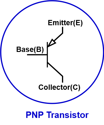
The emitter is heavily doped to provide holes as majority charge carriers, while the base is lightly doped and very thin to ensure efficient carrier movement. The collector is moderately doped and larger in size to handle heat dissipation effectively. The circuit symbol of a PNP transistor is shown in the figure below.
A PNP transistor operates by controlling the flow of current between the emitter and collector, with the base serving as the control terminal. Unlike NPN transistors, which rely on electrons, a PNP transistor primarily utilizes holes for conduction, making its behavior opposite to that of an NPN transistor.
When a negative voltage is applied to the base relative to the emitter, a small current flows from the emitter to the base. This action allows a significantly larger current to flow from the emitter to the collector, making PNP transistors essential for amplification and switching applications in electronic circuits.
The PNP transistor operates in three distinct modes. In the cutoff region, the base-emitter junction is not forward-biased, preventing current flow and keeping the transistor in an OFF state. This means no conduction occurs between the emitter and collector, effectively turning the transistor off.
In the active region, the base-emitter junction is forward-biased, while the base-collector junction is reverse-biased. This condition enables a controlled current flow from the emitter to the collector, making the transistor function as an amplifier, which is crucial in many electronic applications like audio and radio amplifiers.
In the saturation region, the base-emitter junction remains forward-biased, and the base-collector junction becomes slightly forward-biased as well. This allows maximum current flow, meaning the transistor acts as a fully closed switch, enabling its use in digital switching and power control circuits.
PNP transistors find applications in various electronic circuits. They are commonly used in amplifiers to boost audio, radio, and other signal-processing applications. They also play a vital role in switching circuits, such as motor drivers, battery management systems, and relay circuits, where they regulate power flow efficiently.
Additionally, PNP transistors are used in oscillator circuits, sensor applications, and complementary transistor pair designs. Often, they are paired with NPN transistors to form push-pull amplifier circuits, which are widely used in audio amplifiers, power electronics, and analog signal processing for efficient circuit performance.
PNP transistors offer several advantages. They are particularly useful in positive ground configurations, making them suitable for automotive and industrial electronics. Additionally, they exhibit low-noise characteristics, making them ideal for high-fidelity audio applications. Their efficiency in low-power circuits makes them essential in analog and low-frequency applications.
Despite their benefits, PNP transistors have some disadvantages. They typically have slower switching speeds than NPN transistors due to the lower mobility of holes as charge carriers. Furthermore, PNP transistors are less commonly used, as most modern electronic circuits favor NPN transistors due to standard negative ground configurations.
Another limitation of PNP transistors is that they require negative voltages, which complicates integration with standard power supplies. This factor makes circuit design more challenging, particularly when using PNP transistors in systems that predominantly use positive voltage sources for operation and signal processing.
Despite these drawbacks, PNP transistors remain essential in power electronics, signal processing, and analog circuits. Their role in complementary transistor designs, especially in push-pull amplifiers and H-bridge motor control circuits, ensures their continued use in various electronic applications, maintaining their relevance in modern technology.
Difference Between NPN and PNP Transistor
The table below highlights the key differences between NPN and PNP transistor, including their structure, operation, and characteristics:
| Difference | NPN Transistor | PNP Transistor |
|---|---|---|
| Description | An NPN transistor consists of a thin layer of P-type semiconductor sandwiched between two N-type semiconductor layers. | A PNP transistor consists of a thin layer of N-type semiconductor sandwiched between two P-type semiconductor layers. |
| Terminal Polarity | The emitter is N-type, the base is P-type, and the collector is N-type. | The emitter is P-type, the base is N-type, and the collector is P-type. |
| Current Direction | Current flows from the collector to the emitter. | Current flows from the emitter to the collector. |
| Majority Charge Carriers | Electrons are the majority charge carriers. | Holes are the majority charge carriers. |
| Minority Charge Carriers | Holes act as minority charge carriers. | Electrons act as minority charge carriers. |
| Switching Speed | Faster switching due to the high mobility of electrons. | Slower switching due to the low mobility of holes. |
| Switching Time | Short switching time, making it ideal for high-speed applications. | Long switching time, limiting its use in high-frequency applications. |
| Active Region Operation | The emitter is connected to the negative terminal of the power supply, and the collector is connected to the positive terminal with respect to the base. | The emitter is connected to the positive terminal, and the collector is connected to the negative terminal with respect to the base. |
| Saturation Region Operation | When both the emitter and collector are negative with respect to the base, the transistor is in saturation and acts as an ON switch. | When both the emitter and collector are positive with respect to the base, the transistor is in saturation and acts as an ON switch. |
| Cutoff Region Operation | The emitter and collector are positive with respect to the base, preventing conduction. | The emitter and collector are negative with respect to the base, preventing conduction. |
| Ground Signal | Low ground signal required for operation. | High ground signal required for operation. |
| Starting of Conduction | Begins conduction when electrons enter the base region. | Begins conduction when holes enter the base region. |
| Switching ON & OFF | Turned ON by applying a positive voltage at the base; turned OFF by reducing the base voltage. | Turned ON by applying a negative voltage at the base; turned OFF by applying a positive voltage. |
| Direction of Base Current | Base current flows from base to emitter. | Base current flows from emitter to base. |
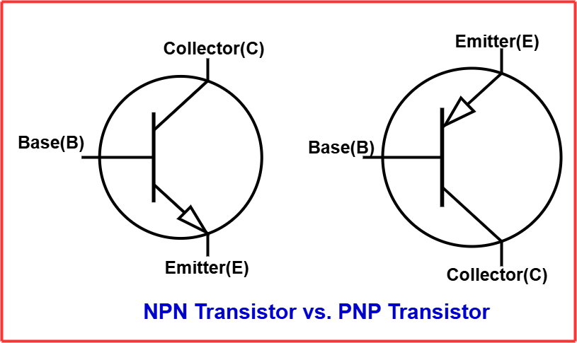
| Emitter Arrow Direction | The emitter arrow points outward in the circuit symbol. | The emitter arrow points inward in the circuit symbol. |
| Application in Circuits | Commonly used in digital electronics, high-speed switching, and power amplification. | Used in low-noise applications, complementary circuits, and motor control circuits. |
| Use in Logic Circuits | Preferred for most logic circuits, including TTL and CMOS, due to faster response. | Less commonly used in logic circuits but found in specific designs like push-pull amplifiers. |
| Voltage Biasing | Requires positive biasing at the base to conduct. | Requires negative biasing at the base to conduct. |
| Popularity | More widely used in modern circuits due to easier compatibility with negative ground systems. | Less frequently used but still essential for complementary circuit designs. |
The NPN transistor is generally preferred for most high-speed switching applications, while the PNP transistor is often used in low-noise amplifiers and complementary transistor circuits.
Conclusion
From the above discussion, it is clear that NPN and PNP transistors have distinct characteristics, including their charge carriers, current flow, and switching behavior. Both types are essential in electronic applications such as switching and amplification. Understanding these differences helps in selecting the appropriate transistor based on specific circuit requirements.
Choosing between an NPN or PNP transistor depends on circuit design, voltage polarity, and application needs. NPN transistors are preferred in high-speed applications due to their faster switching, while PNP transistors are used in certain analog circuits. A clear understanding of their working principles ensures efficient and optimal circuit performance.
Read Next: