A diode clipper, also called a diode limiter, is a wave-shaping circuit that modifies an input signal by removing or limiting portions of its amplitude. Depending on the circuit configuration, diode clipping circuits can clip the positive half-cycle, negative half-cycle, or both halves of the waveform while leaving the remaining portion largely unchanged.
What Are Diode Clipping Circuits?
Diode clipping circuits are wave-shaping circuits that use one or more diodes to limit selected portions of an input voltage waveform. Depending on the circuit arrangement, they can remove or flatten the positive peaks, negative peaks, or both sides of a signal once the voltage reaches a specified clipping level.
When the input exceeds the clipping level, the diode changes from its blocking state to its conducting state. This limits the output voltage and produces a waveform with its peaks partially or completely flattened. A simple half-wave rectifier can also be considered a basic form of clipping because it suppresses one half of the input waveform.
Diode clipping circuits are widely used for waveform shaping, signal limiting, noise suppression, and overvoltage protection. Depending on the required clipping level and application, conventional PN diodes, Schottky diodes, or Zener diodes can be used. Zener-based clippers are particularly useful when a defined voltage limit is required to protect a circuit from excessive voltage spikes.
Main Types of Diode Clipping Circuits
A diode can conduct current when it is forward biased and largely blocks current when it is reverse biased. For a typical silicon diode, a forward voltage of about 0.7 V is commonly used as an approximate value.
A diode clipping circuit uses this one-way conduction property to control selected portions of an input waveform. Depending on how the diode is connected, clipping circuits are mainly classified as series clippers and parallel clippers.
Series Clipper
In a series clipper, the diode is connected in series with the input signal and load. The diode must be forward biased and conducting for the corresponding portion of the input signal to reach the output.
When the diode is reverse biased, it blocks the signal path and prevents that portion of the waveform from appearing at the output.
Parallel Clipper
In a parallel clipper, the diode is connected in a branch parallel to the load. When the diode becomes forward biased, it provides a conducting path that limits the output voltage to the desired level.
The diode orientation determines whether the positive or negative portion of the input waveform is clipped.
A clipping circuit can be used with different types of input waveforms. For basic analysis, a sinusoidal AC waveform is commonly considered because it clearly shows how the diode conducts during one portion of the cycle and blocks during the other.
The main types discussed below are:
- Positive diode clipper
- Negative diode clipper
- Positive and negative clipper
- Biased diode clipper
- Zener diode clipper
This classification makes it easier to understand how changing the diode orientation, bias voltage, and diode type changes the clipping level and the resulting output waveform.
Parallel Positive Diode Clipping Circuit
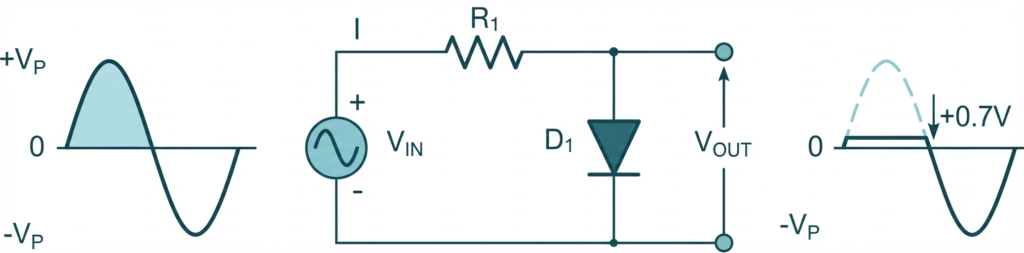
A parallel positive diode clipper is designed to limit the positive portion of an input waveform while allowing the negative portion to pass with little or no clipping.
During the positive half-cycle of the sinusoidal input, the diode becomes forward biased when its anode is more positive than its cathode. For a typical silicon diode, conduction begins when the applied voltage reaches approximately +0.7 V. A germanium diode requires a lower forward voltage, typically around +0.3 V.
Once the diode conducts, it provides a low-resistance path that limits the output voltage to approximately the diode’s forward-voltage level. Therefore, the positive portion of the waveform above the clipping level is removed or flattened.
During the negative half-cycle, the diode becomes reverse biased. It then presents a high impedance to the signal, so it has little effect on the negative portion of the waveform. The negative half-cycle therefore appears at the output with essentially the same shape as the input.
Thus, the circuit clips the positive peaks while allowing the negative portion of the waveform to pass, which is why it is called a positive diode clipper.
For a silicon diode:
The actual clipping voltage depends on the diode’s forward current, temperature, and characteristics.
Parallel Negative Diode Clipping Circuit
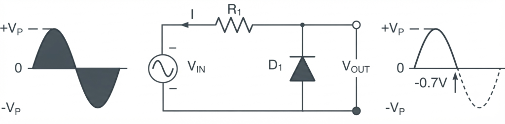
A parallel negative diode clipper works in the opposite manner to a positive clipper. It is designed to restrict the negative portion of the input waveform while allowing the positive portion to pass with little or no clipping.
During the negative half-cycle of the sinusoidal input, the diode becomes forward biased and starts conducting when the input reaches approximately the diode’s forward-voltage level. For a typical silicon diode, the clipping level is approximately −0.7 V.
Once the diode conducts, it provides a low-resistance path that limits the negative portion of the output waveform. As a result, the part of the input signal below the clipping level is removed or flattened.
During the positive half-cycle, the diode is reverse biased and behaves approximately like an open circuit. It therefore has little effect on the positive portion of the waveform, which passes through to the output.
Thus, a parallel negative diode clipper limits the negative peaks of the input signal while allowing the positive portion to pass essentially unchanged.
For a typical silicon diode, the approximate clipping level is:
The actual clipping level depends on the diode’s forward current, temperature, and specific characteristics.
Parallel Clipping of Both Half Cycles
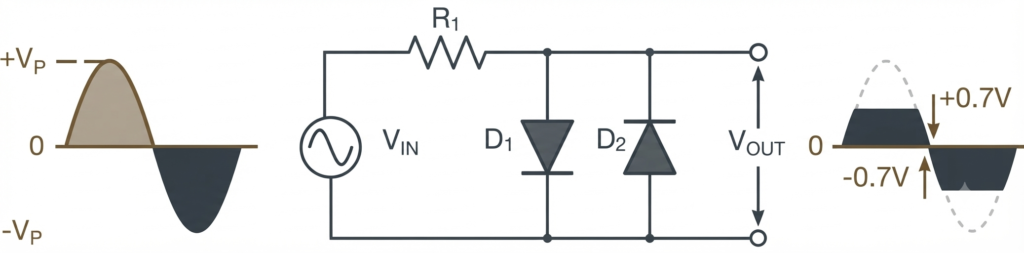
A parallel clipper for both half cycles uses two diodes connected in opposite directions. This arrangement allows one diode to limit the positive half-cycle, while the other limits the negative half-cycle of the input waveform.
During the positive half-cycle, D1 becomes forward biased and clips the positive peak. During the negative half-cycle, D2 conducts and limits the negative peak. Therefore, the same circuit can control both sides of an alternating waveform.
For practical silicon diodes, the forward voltage is approximately 0.7 V under typical operating conditions. Consequently, the clipping levels are approximately: and .
The actual clipping levels depend on the diode’s forward voltage, current, and temperature.
Increasing the Clipping Level
The clipping threshold can be increased beyond ±0.7 V. One simple approach is to connect multiple diodes in series. Each additional silicon diode contributes approximately its forward voltage to the clipping level.
For n identical silicon diodes:
For example, two series-connected silicon diodes would produce an approximate clipping level of:
Another approach is to use a DC bias voltage with the diodes. This allows the clipping level to be selected more precisely rather than being restricted to multiples of the diode’s forward voltage.
Thus, by changing the diode arrangement or adding a suitable bias voltage, a clipping circuit can be designed to limit the positive peak, negative peak, or both peaks at selected voltage levels.
Biased Diode Clipping Circuits
A biased diode clipping circuit uses an additional DC bias voltage to set the clipping level at a value other than the diode’s normal forward-voltage level. This allows the circuit to limit a waveform at a selected voltage rather than simply clipping it near ±0.7 V.
For a positive biased clipper using a silicon diode, the diode begins to conduct when the input voltage exceeds the sum of the applied bias voltage and the diode forward voltage:
Assuming a silicon diode with:
and a bias voltage of:
the approximate clipping level is:
Therefore, when the input voltage rises above approximately +4.7 V, the diode becomes forward biased and begins conducting. The portion of the waveform above this level is consequently clipped or limited.
The advantage of a biased clipper is that the clipping level can be selected according to the requirements of the circuit rather than being fixed near the diode’s natural forward voltage.
Parallel Positive Clipper with Positive Bias
A parallel positive clipper with positive bias combines a diode with a DC bias source to establish a positive clipping level above 0 V. The bias voltage shifts the point at which the diode begins to conduct, allowing the circuit to remove only the portion of the positive waveform that exceeds the selected limit.
When the input voltage rises above the combined bias voltage and diode forward voltage, the diode becomes forward biased and conducts. For a silicon diode, the clipping level can be approximated as:
For example, with a 4 V bias and a 0.7 V silicon-diode forward voltage:
Therefore, positive portions of the input waveform above approximately +4.7 V are clipped, while lower voltage portions remain essentially unaffected.
By reversing the diode orientation and bias polarity, the circuit can instead limit the negative portion of the waveform. In that arrangement, the negative clipping level is approximately:
For a 4 V bias and a 0.7 V forward voltage, the negative clipping level would be approximately −4.7 V. This arrangement is useful when a signal must be restricted to a defined negative voltage limit.
Parallel Negative Clipper with Negative Bias
A parallel negative clipper with negative bias is designed to limit the negative portion of an input waveform at a selected voltage level. The added negative bias shifts the clipping point below 0 V, allowing the circuit to control the negative peak more precisely than an unbiased diode clipper.
When the input voltage becomes sufficiently negative, the diode becomes forward biased and starts conducting. For a silicon diode, the negative clipping level can be approximated by:
For example, if the magnitude of the bias voltage is 4 V and the diode forward voltage is approximately 0.7 V:
Thus, negative portions of the input waveform below approximately −4.7 V are clipped, while the positive portion is allowed to pass with little effect.
Independent Positive and Negative Clipping Levels
The clipping levels can be adjusted independently by using two biased diodes—one for the positive peaks and another for the negative peaks. The two bias voltages do not have to be equal.
For example, a circuit could be designed with:
- Positive bias: 4 V
- Negative bias: 6 V
Using a silicon diode with an approximate forward voltage of 0.7 V, the corresponding clipping levels would be approximately: and
This arrangement allows the circuit to pass the central portion of the waveform while limiting positive peaks above +4.7 V and negative peaks below −6.7 V. Such independently adjustable clipping levels are useful when a signal must remain within different positive and negative voltage limits.
Zener Diode Clipping Circuits
A Zener diode clipper provides a practical way to limit a signal without requiring a separate DC bias supply. Instead of using an external voltage source to establish the clipping point, the circuit takes advantage of the Zener diode’s controlled reverse-breakdown characteristic.
A Zener diode is designed to withstand operation in the reverse-breakdown region. When the reverse voltage reaches its specified Zener voltage (Vz), the device begins conducting and maintains a voltage close to its rated breakdown value over its intended operating range. This characteristic makes it useful for both voltage regulation and signal-limiting applications.
In the forward direction, a Zener diode behaves similarly to a conventional silicon diode. For basic calculations, its forward voltage can be taken as approximately 0.7 V. In the reverse direction, it initially blocks current until the applied voltage reaches the Zener breakdown level. Beyond this point, the current increases significantly while the voltage remains approximately at the Zener voltage.
This behavior allows a Zener diode to limit excessive portions of an input waveform. The Zener voltage establishes the main reverse clipping level, making the circuit useful for signal protection, voltage limiting, and suppression of unwanted voltage peaks.
In a practical Zener clipping circuit, the limiting voltage depends on the Zener voltage, forward voltage, operating current, and circuit configuration. Therefore, the actual clipping level should be determined from the Zener diode’s datasheet rather than assuming an ideal constant value.
Zener Diode Clipping
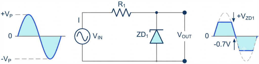
A Zener diode clipping circuit uses the reverse-breakdown characteristic of a Zener diode to limit the amplitude of an input waveform. The Zener voltage effectively acts as the reference level that determines when the diode starts conducting in reverse bias.
During the positive half-cycle, the Zener diode is reverse biased. When the input voltage reaches the specified Zener voltage (Vz), the diode enters its breakdown region and limits the output voltage to approximately that level.
During the negative half-cycle, the Zener diode becomes forward biased and behaves like a conventional silicon diode. Its forward voltage is typically around 0.7 V under normal operating conditions.
Therefore, the clipping levels of a simple Zener clipper can be approximately represented as: and .
Full-wave Zener Diode Clipping
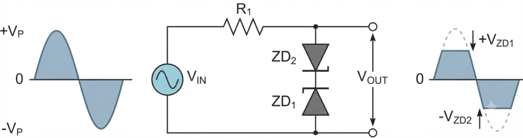
The same principle can be extended to both positive and negative peaks by connecting two Zener diodes back-to-back in series. During one half-cycle, one Zener operates in reverse breakdown while the other is forward biased. Their roles reverse during the opposite half-cycle.
As a result, the circuit can limit both halves of the input waveform. The clipping level is approximately determined by the Zener breakdown voltage plus the forward voltage of the other diode:
For a silicon diode with V_F ≈ 0.7 V, the clipping level is therefore approximately Vz + 0.7 V on each side, depending on the circuit polarity and Zener ratings.
Applications of Clipping Circuits
Clipping circuits are widely used in electronic systems to control signal amplitude, remove unwanted portions of waveforms, and protect circuits from excessive voltage. Some important applications include:
- Noise reduction: Clipping circuits can be used in FM transmitters to limit unwanted amplitude variations and reduce the effect of noise on the signal.
- Voltage limiting: They limit the input or output voltage to a predetermined level, preventing excessive voltage from reaching sensitive electronic components.
- Waveform shaping: A clipping circuit can remove selected portions of a waveform to produce a required output shape. This is useful in signal-processing and pulse-generation circuits.
- Overvoltage protection: Clipping circuits can protect electronic devices and circuit inputs by restricting voltage spikes to a safe range.
- Signal conditioning: They are used to control the amplitude of signals before they are applied to amplifiers, comparators, logic circuits, or other processing stages.
- Pulse generation: By clipping portions of a sinusoidal or other periodic waveform, clipping circuits can help produce pulse-like or rectangular waveforms.
- Amplitude control: Diode clippers can restrict positive peaks, negative peaks, or both, making them useful where a signal must remain within specified voltage limits.
- Waveform restoration and processing: Clipping can be used as part of signal-processing circuits where unwanted portions of an input waveform need to be removed.
- Communication circuits: Clipping circuits are used in communication systems for limiting signal levels and controlling unwanted amplitude variations.
- Electronic protection circuits: Biased and Zener clipping circuits can provide specific positive and negative voltage limits, making them useful for protecting circuit inputs from abnormal signal levels.
Conclusion
Diode clipping circuits are useful wave-shaping circuits that limit selected portions of an input signal to a desired voltage level. Depending on the circuit arrangement, they can clip the positive peaks, negative peaks, or both portions of a waveform.
The clipping level can be controlled by the diode’s forward voltage, an external bias voltage, or the breakdown voltage of a Zener diode. This makes diode clippers useful for signal limiting, voltage protection, noise suppression, and waveform shaping.
A clipping circuit does not have to be limited to sinusoidal signals. The same principle can be applied to different waveform shapes whenever a portion of the signal needs to be restricted or removed.
It is also important to distinguish a clipper from a clamper. A clipper restricts part of the waveform amplitude, whereas a clamper shifts the waveform’s DC level without primarily changing its overall shape.
Overall, the diode’s ability to conduct in one direction and block in the other makes it a simple and effective component for controlling signal amplitude and protecting electronic circuits.
Read Next:
- Schottky Diode vs Zener Diode
- Difference Between BJT and MOSFET
- Difference Between Diode and Rectifier
- Difference Between Diode and Transistor
- Difference Between Silicon Diode and Germanium Diode
- Diode Voltage Drop: Formula, Values, Chart, Table & Measurement
- Diode Turn-On Voltage: Definition, Values & Examples