Discover the NPN transistor, its definition, construction, and working principle. Learn how NPN transistors function, their applications, advantages, and characteristics in electronic circuits.
A Bipolar Junction Transistor (BJT) is a semiconductor device that utilizes both electrons and holes as charge carriers to facilitate current flow. It allows a small input current at one terminal to regulate a larger current between the other two terminals, making it ideal for switching and amplification applications.
BJTs are classified into two main types:
- PNP Transistor
- NPN Transistor
A PNP transistor consists of three layers of semiconductor material, where two P-type regions enclose a central N-type region. This structure enables current flow primarily through holes, making it function differently from an NPN transistor, which relies on electron movement.
NPN Transistor
The NPN transistor consists of two N-type semiconductor layers with a P-type layer in between. In this structure, electrons act as the majority charge carriers, while holes serve as the minority charge carriers. This configuration ensures efficient current flow, making NPN transistors highly suitable for amplification and switching applications.
The circuit symbol of an NPN transistor features an arrow on the emitter pointing outward, signifying the conventional current flow from collector to emitter when the transistor is active. Due to their high-speed switching capability and effective signal amplification, NPN transistors are widely used in modern electronic circuits. The symbol of NPN transistor is given in the figure below.

In the above figure, we can see an arrow pointing outward from the emitter terminal. This indicates the direction of the flow of current through the device.
Construction of NPN Transistor
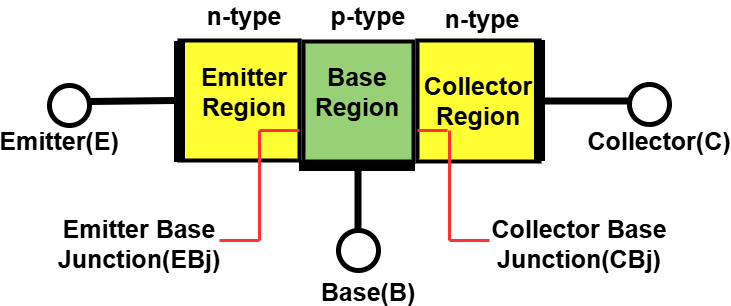
The NPN transistor is constructed using semiconductor materials such as silicon or germanium. It is formed when a P-type semiconductor layer is placed between two N-type semiconductor layers, creating a three-layered structure essential for its operation.
This transistor consists of three terminals: emitter, base, and collector. It also contains two diodes connected back-to-back. The diode between the emitter and base is called the emitter-base diode, while the diode between the collector and base is known as the collector-base diode. In terms of doping levels, the emitter is moderately doped, the base is lightly doped, and the collector is more heavily doped, ensuring efficient charge carrier movement and device performance.
The NPN transistor operates by controlling the flow of electrons, which serve as the majority charge carriers. When a small current is applied to the base terminal, it allows a larger current to flow from the emitter to the collector. This property makes NPN transistors highly efficient for amplification and switching applications in electronic circuits.
The doping levels in an NPN transistor play a crucial role in its functionality. The lightly doped base ensures minimal recombination of charge carriers, allowing most electrons from the emitter to pass into the collector. This design enhances the current gain (β), making the transistor highly effective for signal processing, power regulation, and high-frequency applications.
Working of NPN Transistor
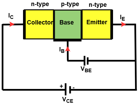
An NPN transistor operates based on charge carrier movement within its three regions: emitter, base, and collector. The emitter-base junction is forward-biased, applying a small voltage (VBE) to reduce the barrier potential. Meanwhile, the collector-base junction is reverse biased with a higher voltage (VCE) to attract charge carriers efficiently.
When the emitter-base junction is forward-biased, electrons from the heavily doped emitter gain energy and move toward the base. The base, being thin and lightly doped, has few holes available for recombination. As a result, only a small fraction of electrons combine with holes, generating a very small base current (IB).
Most electrons move past the base and enter the collector due to the reverse-biased collector-base junction. This strong electric field in the collector attracts the electrons, allowing a large collector current (IC) to flow. The transistor operates efficiently because most charge carriers pass through with minimal recombination in the base region.
The total emitter current (IE) is the sum of the base current (I_B) and the collector current (IC), expressed as IE = IB + IC. Since the base current is very small compared to the emitter and collector currents, an NPN transistor achieves current amplification, making it useful in many applications.
The amplification capability of the NPN transistor is measured using the current gain factor, β (beta), which is the ratio of collector current to base current (β = IC/IB). This gain factor typically ranges from 20 to 1000, depending on the transistor type, making it effective for amplifying weak electrical signals.
An NPN transistor functions in different regions based on its biasing conditions. In the active region, it acts as an amplifier where the collector current is proportional to the base current. In the saturation region, it behaves like a closed switch, allowing maximum current flow. In cutoff, the transistor remains off.
These operational modes make NPN transistors essential in various applications. They are widely used in signal amplification circuits, switching applications in microcontrollers, logic gates, and power electronics. Their efficiency in handling high-speed switching and current control makes them ideal for use in modern digital and analog electronic circuits.
NPN Transistor as a Switch
An NPN transistor can function as an efficient electronic switch by regulating the current flow between the collector and emitter terminals. This switching capability is widely utilized in digital circuits, motor control, and power management applications. By adjusting the base current, we can control whether the transistor is in an “ON” or “OFF” state, thereby allowing or blocking current flow through the load connected to the collector.
In the ON state (saturation region), a small current is applied to the base, allowing a much larger current to flow from the collector to the emitter. When the base-emitter junction is forward biased (VBE ≈ 0.7V for a silicon transistor), the transistor enters saturation, meaning it acts as a closed switch with very low resistance. In this condition, the voltage drop across the transistor (VCE) is minimal, and most of the supply voltage is delivered to the connected load.
In the OFF state (cut-off region), no base current is supplied, preventing the flow of current between the collector and emitter. In this state, the transistor behaves as an open switch with high resistance, blocking the circuit and preventing current from passing through. This makes it highly effective for applications where a binary ON/OFF control mechanism is required.
By properly selecting the base resistor and ensuring the transistor operates in either complete saturation or cut-off, we can achieve efficient and reliable switching. This principle is commonly used in transistor-based logic circuits, relay drivers, LED controls, and other electronic applications where switching functionality is required.
NPN Transistor Amplifier in Common Emitter Configuration
In addition to functioning as a semiconductor switch that turns load currents “ON” or “OFF” by controlling the base signal in saturation or cut-off regions, an NPN transistor can also operate in its active region. In this state, it amplifies small AC signals applied to its base terminal while keeping the emitter grounded.
By applying a suitable DC biasing voltage to the base terminal, the transistor operates within its linear active region, forming an inverting amplifier circuit known as a single-stage common emitter amplifier. This configuration allows for effective signal amplification, making it a crucial component in electronic circuits.
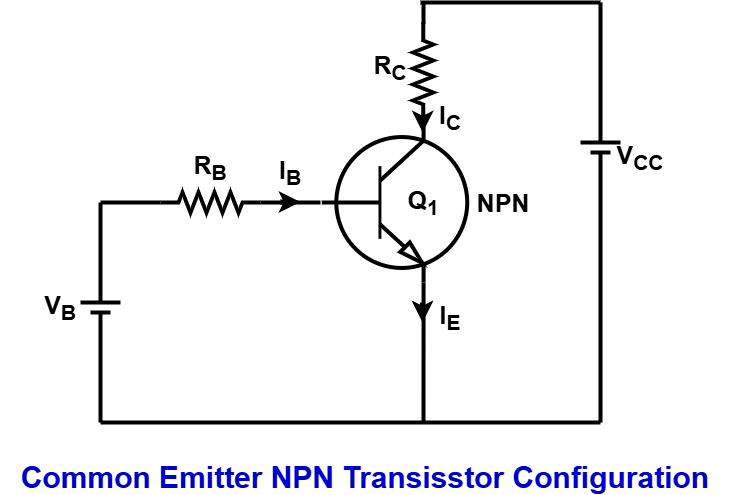
One well-known common emitter amplifier configuration using an NPN transistor is called a Class A Amplifier. In this setup, the base terminal is biased to keep the base-emitter junction forward-biased. As a result, the transistor operates between cut-off and saturation, enabling accurate reproduction of both halves of an AC input signal.
Without this bias voltage, only one-half of the input waveform would be amplified, leading to signal distortion. Due to its ability to amplify complete waveforms, the common emitter amplifier is widely used in various applications, particularly in audio circuits such as pre-amplifier and power amplifier stages.
The output characteristics of a common emitter amplifier are represented by a set of curves known as output characteristic curves. These curves depict the relationship between the collector current (IC) and the collector-emitter voltage (VCE) for different values of base current (IB), providing insight into the transistor’s performance.
A DC load line is drawn on these curves to represent all possible operating points based on different base current values. Properly setting the collector-emitter voltage (VCE) ensures the transistor can amplify AC signals effectively. This optimal point is known as the quiescent point (Q-point), ensuring stable operation.
Input Characteristics of an NPN transistor
The input characteristics of an NPN transistor represent the relationship between the base current (IB) and the base-emitter voltage (VBE) for a fixed collector-emitter voltage (VCE).
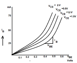
This characteristic curve helps in understanding how the base current varies with changes in the base-emitter voltage while keeping the collector-emitter voltage constant. It is similar to the forward bias characteristics of a PN junction diode since the base-emitter junction behaves like a diode.
Output Characteristics Curves of a NPN Transistor
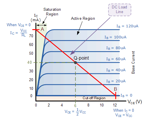
The most crucial observation is the effect of the collector-emitter voltage (VCE) on the collector current (IC) when VCE exceeds approximately 1.0 volt. Beyond this point, IC remains relatively constant despite changes in VCE and is primarily controlled by the base current (IB). This behavior signifies that the output circuit functions as a “Constant Current Source.”
From the common emitter circuit, we can see that the emitter current (IE) is the sum of the collector current (IC) and the base current (I_B). Mathematically, this relationship is expressed as IE = IC + IB. This fundamental equation defines current flow in the common emitter (CE) configuration and is crucial in transistor analysis.
Using the output characteristic curves and Ohm’s Law, the current flowing through the load resistor (RL) is equal to the collector current (IC). This corresponds to the supply voltage (VCC) minus the voltage drop across the collector-emitter terminals (VCE). The equation governing this behavior helps determine the transistor’s performance under varying conditions.
A straight line, known as the Dynamic Load Line, can be plotted on the characteristic curves. This line extends from the saturation point (A), where VCE = 0, to the cut-off point (B), where IC = 0. The intersection of this line with the transistor’s characteristic curves defines the transistor’s operating point, or Q-point. Any position along this line represents the transistor’s active region, where amplification occurs.
The collector characteristics of an NPN transistor can be used to predict the collector current (IC) for a given VCE and base current (IB). A load line can be drawn on these curves to determine a suitable operating Q-point, which can be adjusted by varying the base current. The slope of this load line is determined by the reciprocal of the load resistance (-1/RL).
An NPN transistor is typically “OFF” in its default state. However, a small base current combined with a positive base voltage relative to the emitter turns it “ON,” allowing a much larger collector-emitter current to flow. This property makes NPN transistors essential in amplification and switching applications.
α and β Relationship in a NPN Transistor
In an NPN transistor, the relationship between α (alpha) and β (beta) is crucial in determining its current gain and amplification properties. Alpha (α) is known as the common-base current gain, which represents the ratio of the collector current (IC) to the emitter current (IE). It is given by the formula α = IC / IE and typically has a value between 0.95 and 0.99, meaning that almost all the emitter current flows into the collector.
On the other hand, beta (β) is the common-emitter current gain, which defines how much the transistor amplifies the base current. It is expressed as β = IC / IB, where IB is the base current. The value of β is generally much greater than α, typically ranging from 20 to 1000, depending on the transistor type. This high value of β makes NPN transistors highly efficient for amplification and switching applications.
The relationship between α and β is mathematically expressed as β = α / (1 – α), and conversely, α = β / (β + 1). This equation shows that even a small change in the base current significantly affects the collector current, demonstrating why NPN transistors are widely used in circuits where signal amplification is required.
Key Regions of an NPN Transistor
Emitter Region: The emitter is the largest section of the transistor structure, larger than the base but smaller than the collector. It is heavily doped to ensure a high concentration of majority charge carriers, which are electrons. The emitter is forward-biased relative to the base, allowing efficient injection of electrons into the base region.
Base Region: Positioned between the emitter and collector, the base is the smallest and thinnest region of the transistor. It is lightly doped to minimize recombination, ensuring that most of the injected electrons pass through to the collector. This design allows for efficient amplification and current transfer within the transistor.
Collector Region: The collector is the largest section of the transistor, designed to collect the majority carriers from the base region. It is lightly doped compared to the emitter but has a larger physical size to dissipate heat effectively. The collector is reverse biased with respect to the base, facilitating efficient charge carrier collection and current flow.
Applications of NPN Transistor
NPN transistors are extensively used in various electronic applications due to their efficiency in amplification and switching. One of their primary uses is in switching circuits, where they act as electronic switches to control the flow of current. Their ability to handle fast switching speeds makes them ideal for digital logic circuits.
These transistors are also commonly used in Darlington pair circuits, which amplify weak signals by increasing current gain. This configuration is particularly useful in sensor applications and low-power signal amplification. Additionally, NPN transistors play a crucial role in circuits that require current sinking, efficiently directing current flow to the ground.
In amplifier applications, NPN transistors are used in classic configurations such as push-pull amplifier circuits, which improve power efficiency and reduce distortion. They are also found in temperature-sensing circuits, where their electrical properties change in response to temperature variations, making them useful for monitoring and regulation systems.
Another significant application of NPN transistors is in logarithmic converters, which are used in signal processing and measurement systems. These converters utilize the transistor’s exponential voltage-current relationship to perform logarithmic transformations, essential in applications such as audio compression and analog computation.
Advantages of NPN Transistors
- Compact Size: NPN transistors are small, making them ideal for modern miniaturized electronic devices and integrated circuits.
- High Amplification Efficiency: They provide efficient signal amplification, making them perfect for audio, RF, and general electronic applications.
- Fast Switching Speed: NPN transistors support high-speed switching, making them suitable for digital circuits, microcontrollers, and processors.
- Cost-Effective: These transistors are affordable and widely used in various consumer and industrial electronics.
- Versatile Applications: Their flexibility allows them to be configured in multiple circuit designs, including switching, amplification, and voltage regulation.
Disadvantages of NPN Transistors
- Signal Inversion: The output signal is often inverted compared to the input, requiring additional circuitry for correction in some applications.
- Heat Dissipation Issues: NPN transistors generate heat during operation, necessitating cooling mechanisms like heat sinks in high-power applications.
- Temperature Sensitivity: Their performance can be affected by temperature variations, impacting circuit stability.
- Complex Circuit Design: Advanced applications require precise biasing and complex circuit designs, making them challenging for beginners.
- Limited Power Handling: In high-power applications, alternatives like MOSFETs are often preferred due to better efficiency and power-handling capabilities.
Conclusion
NPN transistors are essential components in modern electronics, widely used for switching, amplification, and signal processing. Their compact size, high-speed operation, and cost-effectiveness make them ideal for various applications, from audio amplifiers to microcontrollers.
Despite challenges like heat dissipation and signal inversion, their versatility and efficiency make them a preferred choice in circuit design. Understanding their working principles, configurations, and characteristics helps engineers and hobbyists utilize NPN transistors effectively in electronic circuits, communication systems, and power applications.
Read Next: