Learn about junction transistors, including their types (NPN & PNP), working principles, construction, and applications in amplification and switching. Understand how Bipolar Junction Transistors (BJTs) operate using charge carriers for efficient electronic circuit design.
In 1951, William Shockley invented the first junction transistor, consisting of two back-to-back p-n junctions. This breakthrough revolutionized electronics, paving the way for modern semiconductor devices. Over the years, various transistor types were developed. To distinguish these traditional junction transistors from newer versions, they became known as Bipolar Junction Transistors (BJTs).
Junction transistors played a crucial role in early electronics, enabling advancements in amplification, switching, and signal processing, and are still widely used today in many analog and digital applications.
A junction is a point in an electrical circuit where current can divide or merge. Unlike nodes, which include both connection points and the connecting wires, junctions are specific points of contact without the surrounding wires. Electrical junctions form when multiple conductors or semiconductors come into contact, influencing current flow and electrical properties.
What is a junction?
There are various types of electrical junctions, each serving different functions. Examples include thermoelectric junctions, which generate voltage due to temperature differences, metal-semiconductor junctions used in Schottky diodes, and p-n junctions, which are fundamental to semiconductor devices like diodes and transistors. These junctions play a crucial role in modern electronic circuits.
Understanding Junction Transistors
A BJT functions by controlling the current flow between the collector and emitter terminals through a small current applied to the base terminal. This characteristic makes BJTs highly effective for signal amplification, where a small input current at the base can regulate a much larger output current, making them essential in analog circuits.
There are two main types of BJTs: NPN and PNP transistors. In an NPN transistor, electrons serve as the majority charge carriers, while in a PNP transistor, holes are the dominant charge carriers. The difference in charge carriers affects their operation, making NPN transistors more commonly used due to their faster switching speed and higher efficiency in modern electronic circuits.
Working of Junction Transistors
Compared to the emitter and collector, the base of a transistor is thin and lightly doped, meaning it has a lower density of majority carriers than the emitter and collector. This design ensures efficient charge carrier movement, allowing the transistor to function effectively in amplification and switching applications.
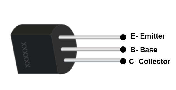
The emitter supplies the current flow, while the collector gathers it. The base acts as a bridge, facilitating the interaction between them for proper connectivity. In a junction transistor, the arrow in the circuit symbol represents conventional current flow. In an NPN transistor, the emitter arrow points away from the base, whereas in a PNP transistor, it points toward the base.
For normal transistor operation in a circuit, the base-emitter junction is typically forward-biased, enabling current flow, while the base-collector junction is reverse-biased, preventing unwanted current leakage and ensuring proper transistor functionality.
The thin and lightly doped base plays a crucial role in transistor operation by allowing most charge carriers from the emitter to pass through to the collector with minimal recombination. This ensures efficient current amplification, as only a small base current is required to control a much larger current between the emitter and collector.
In a functioning transistor circuit, the emitter-base junction is forward-biased, reducing resistance and allowing charge carriers to flow easily. Meanwhile, the base-collector junction remains reverse-biased, creating a potential barrier that directs most charge carriers toward the collector. This mechanism enables the transistor to act as an amplifier or switch, depending on the circuit configuration.
Two Types of Bipolar Junction Transistors
There are two main types of junction transistors: NPN transistor and PNP transistor. These transistors differ based on the arrangement of their semiconductor layers and the type of charge carriers responsible for current flow.
In an NPN transistor, the p-type material forms the base, while the n-type materials form the emitter and collector. Here, electrons act as the majority charge carriers, allowing current to flow from the collector to the emitter when a positive voltage is applied to the base.
Conversely, in a PNP transistor, the n-type material forms the base, while the p-type materials form the emitter and collector. In this case, holes serve as the majority charge carriers, and current flows from the emitter to the collector when a negative voltage is applied to the base.
NPN transistor
In an NPN transistor, the p-type semiconductor base is positioned between an n-doped emitter and an n-doped collector. These transistors are widely used in electronic circuits because electrons, the majority charge carriers in NPN transistors, have higher mobility compared to holes, making them more efficient for signal amplification and switching applications.
The NPN transistor’s construction and symbol highlight its working principle.
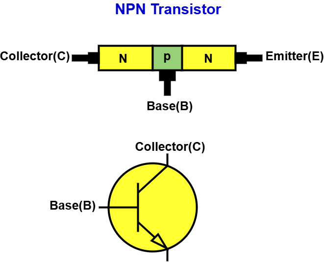
The majority charge carriers in an NPN transistor are electrons, while holes serve as the minority charge carriers. When a small current is applied to the base terminal, it enables a large current to flow from the emitter to the collector, a key property that makes NPN transistors useful in signal amplification.
In forward-biased operation, the emitter-base junction is forward-biased, and the base-collector junction is reverse-biased. The majority charge carriers in the emitter are repelled towards the base, where only a small fraction of electrons recombine with holes. The remaining electrons cross into the collector region, resulting in a larger current flow, making the NPN transistor highly effective for amplification and switching functions.
The thin and lightly doped base of an NPN transistor plays a crucial role in its operation. Since the base is narrow and has fewer charge carriers, most of the electrons injected from the emitter pass through it without recombining. This property allows for efficient current amplification, as a small base current controls a much larger collector current. The ratio of these currents, known as the current gain (β), determines the transistor’s amplification capability.
Additionally, in cut-off and saturation modes, an NPN transistor functions as a switch. In the cut-off region, the base-emitter junction is not forward-biased, preventing current flow and keeping the transistor OFF. In the saturation region, both the emitter-base and base-collector junctions are forward-biased, allowing maximum current flow and turning the transistor ON. These properties make NPN transistors highly suitable for digital logic circuits, microcontrollers, and power electronics.
PNP transistor
A PNP transistor is a type of bipolar junction transistor (BJT) where an n-type semiconductor base is placed between a p-doped emitter and a p-doped collector. Unlike NPN transistors, which use electrons as majority carriers, PNP transistors rely on holes for charge movement. These transistors are widely used in circuits requiring negative voltage control.
The PNP transistor symbol and structure highlight its operation.
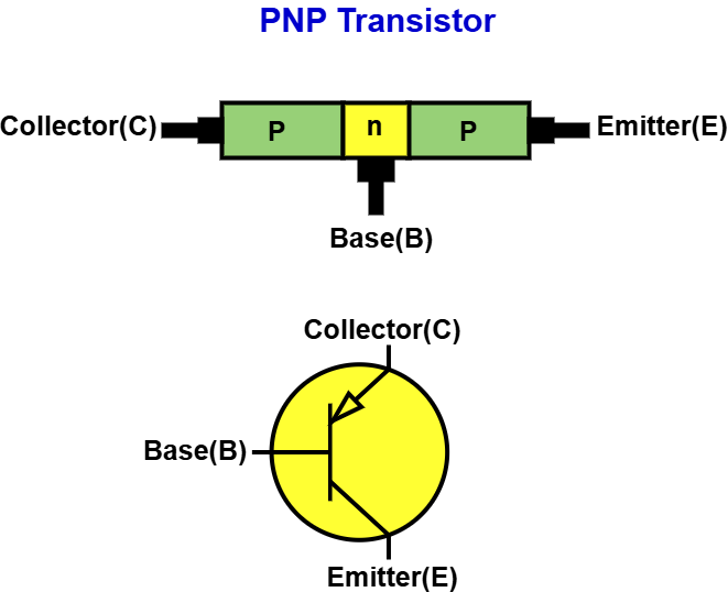
The majority charge carriers in a PNP transistor are holes, while electrons serve as the minority charge carriers. When a small current flows out of the base, it allows a larger current to flow from emitter to collector. This makes PNP transistors efficient for signal amplification in negative power supply circuits.
In active operation, the PNP transistor’s emitter-base junction is forward-biased, and the base-collector junction is reverse-biased. The holes from the emitter move towards the base, where some recombine with electrons. The remaining holes cross into the collector region, enabling a larger current flow, making PNP transistors effective for switching and amplification applications.
The base of a PNP transistor is thin and lightly doped, ensuring efficient charge carrier movement. Since the base is narrow, most of the holes injected from the emitter pass through without recombining. This allows for high current amplification as a small base current controls a much larger collector current, determining the transistor’s current gain (β) and amplification capacity.
In cut-off and saturation modes, the PNP transistor functions as a switch. In the cut-off region, the base-emitter junction is not forward-biased, preventing current flow and keeping the transistor OFF. In the saturation region, both emitter-base and base-collector junctions are forward-biased, allowing maximum current flow and turning the transistor ON for power and signal control.
These switching properties make PNP transistors ideal for power management, signal processing, and analog circuits. They are often used with NPN transistors in complementary transistor circuits to create push-pull amplifiers, motor drivers, and power regulation systems. Understanding PNP transistor operation helps engineers design efficient electronic circuits for power control and signal amplification applications.
Read Next: