A Schottky diode, also known as a Schottky barrier diode, is a type of semiconductor device that has low forward voltage drop and fast switching speed. In this article, we will discuss Schottky diodes in detail, including their working, symbol, characteristics, and applications.
What is a Schottky Diode?
A Schottky diode, also called a Schottky barrier diode, is a special type of diode designed for high-speed switching and low power loss. Unlike standard diodes that use a p-n junction, the Schottky diode forms a junction between a metal and an n-type semiconductor. This unique structure creates a barrier known as the Schottky barrier. This gives the diode a significantly lower forward voltage drop, typically between 0.15 to 0.45 volts, compared to 0.7 volts in silicon diodes.
The low forward voltage drop reduces power loss, making Schottky diodes highly efficient. They are widely used in circuits where speed and efficiency are critical, such as in rectifiers, voltage clamping, and RF systems. Another key feature is their fast recovery time, which enables them to operate effectively in high-frequency applications.
Due to their characteristics, Schottky diodes are commonly used in power supply circuits, solar panels, and automotive systems. However, they have a higher reverse leakage current and lower reverse voltage ratings than traditional diodes. Despite these limitations, the Schottky diode offers efficiency, speed, and functionality for diverse applications.
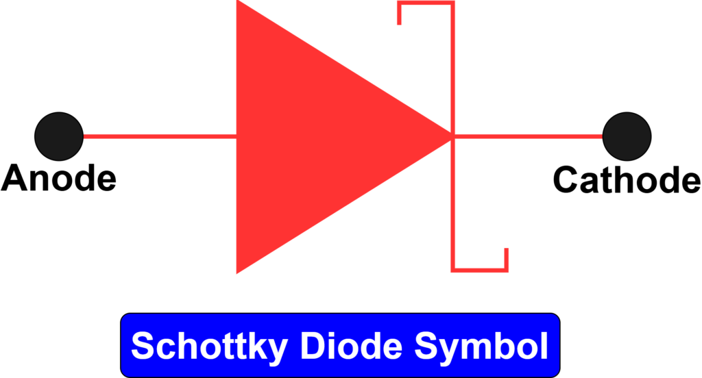
What is the Schottky Diode Symbol?
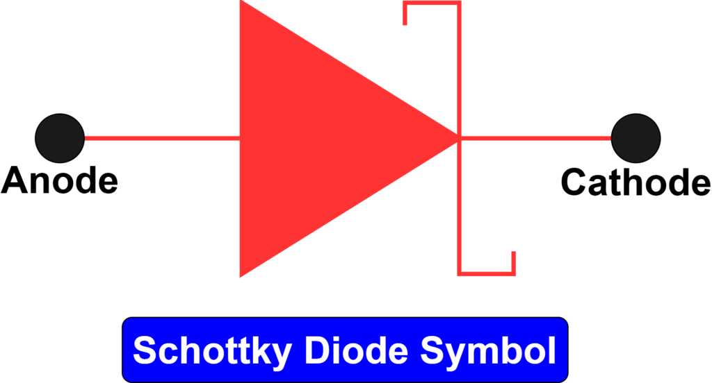
The Schottky diode symbol is slightly different from the standard diode symbol. It features a diode-like triangle pointing towards a vertical line, with an additional curve on the cathode side to signify the metal-semiconductor junction. This symbol of a Schottky diode helps differentiate it from a conventional diode in circuit diagrams.
Schottky Diode Construction
The construction of a Schottky diode involves a metal-semiconductor junction. A metal layer (commonly platinum, molybdenum, or tungsten) is connected to an n-type semiconductor. The metal layer serves as the anode and offers a low resistance for electrons to flow into the semiconductor. The Schottky diode eliminates the p-n junction and allows faster electron flow.
The construction of a Schottky diode differs from that of traditional PN junction diodes. Schottky diodes have a metal layer made of materials like platinum, tungsten, or molybdenum. The cathode is an n-type semiconductor (silicon) that forms a junction with the metal layer. The junction formed between the metal and semiconductor is not a p-n junction but a Schottky barrier. The Schottky barrier changes the electrical characteristics.
Unlike conventional PN junctions, Schottky diodes do not have a significant depletion layer. This results in minimal carrier recombination, lower forward voltage drop, and faster switching speeds. The barrier height at the metal-semiconductor interface determines the diode’s performance. This barrier height controls the flow of electrons from the metal into the semiconductor and allows efficient conduction with minimal power loss.
During diode fabrication, metal is deposited onto the semiconductor surface forming a direct interface. This design eliminates the need for doping which makes Schottky diodes simpler to manufacture compared to traditional silicon-based diodes.
Working of a Schottky Diode
Unlike a standard p-n junction diode, a Schottky diode uses electrons as the majority carriers in both the metal and the semiconductor regions. This unique carrier behavior sets it apart from conventional p-n diodes. The operation of a Schottky diode is detailed for each phase below.
Unbiased Schottky Diode: In an unbiased state, the Schottky diode is not connected to any external voltage source. As a result, there is no potential difference across its terminals.
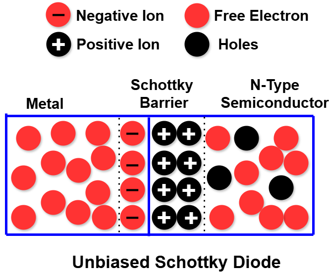
A Schottky diode is formed by combining a metal and an n-type semiconductor. Metals contain free electrons but remain electrically neutral overall. In contrast, the n-type semiconductor has an abundance of free electrons, giving it a negative charge.
When the diode is formed, electrons from the semiconductor move across the junction into the metal. When a neutral atom gains an electron, it becomes negatively charged, and when it loses an electron, it becomes positively charged. As a result, a layer of negatively charged atoms forms on the metal side of the junction, while a layer of positively charged atoms develops on the semiconductor side. This arrangement creates a region known as the Schottky barrier, consisting of opposite charges across the junction.
The Schottky barrier in a Schottky diode acts as a voltage barrier for charge carriers in the semiconductor. This barrier has a built-in potential, which is the minimum voltage required to enable conduction through the junction. The width of this barrier determines the value of the built-in potential.
Because the metal contains a high density of free electrons, the barrier width on the metal side is negligible compared to the n-type semiconductor side. As a result, the built-in potential, or built-in voltage, is very small.
To allow charge carriers to flow through the junction, the applied voltage must exceed this built-in potential. This characteristic leads to the Schottky diode’s low forward voltage drop, making it highly efficient in operation.
Forward Biased Schottky Diode: In forward bias, the metal side of the Schottky diode is connected to the positive terminal of the battery, while the n-type semiconductor side is connected to the battery’s negative terminal.
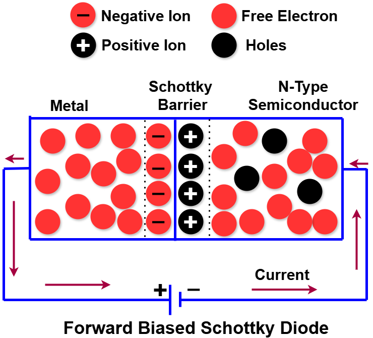
When a voltage is applied, free electrons are produced in the semiconductor region. However, these electrons cannot cross the barrier unless the applied voltage exceeds the built-in potential. In most Schottky diodes, this barrier voltage is approximately 0.2V. Once the applied voltage surpasses 0.2V, the electrons gain sufficient energy to overcome the barrier. As the voltage continues to increase, the depletion region narrows and eventually disappears.
Reverse Biased Schottky Diode: In the reverse-biased state, the negative terminal of the power source is connected to the metal side of the Schottky diode, and the positive terminal is attached to the n-type semiconductor. This configuration creates a potential barrier whose width grows as the reverse voltage increases. Although the reverse bias prevents significant current flow, a small leakage current still exists. As the reverse voltage rises, the leakage current may increase slightly, but it remains limited. If the reverse voltage surpasses a critical threshold, the barrier undergoes permanent breakdown, allowing substantial current to flow in the reverse direction. This breakdown can cause irreversible damage to the device.
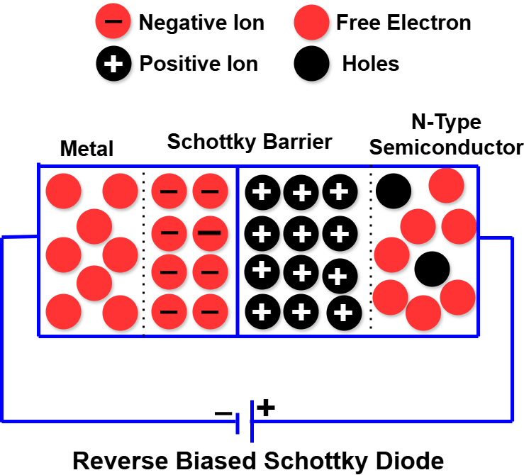
The Schottky diode has an exceptionally short recovery time compared to a PN junction diode. This is because its current flow is solely governed by the movement of the majority charge carriers, which are electrons. As a result, it swiftly ceases conduction as soon as the voltage polarity is reversed.
V-I Characteristics of Schottky Diode
The V-I characteristics of a Schottky diode show the relationship between the voltage and current across the diode. The figure below shows these characteristics.
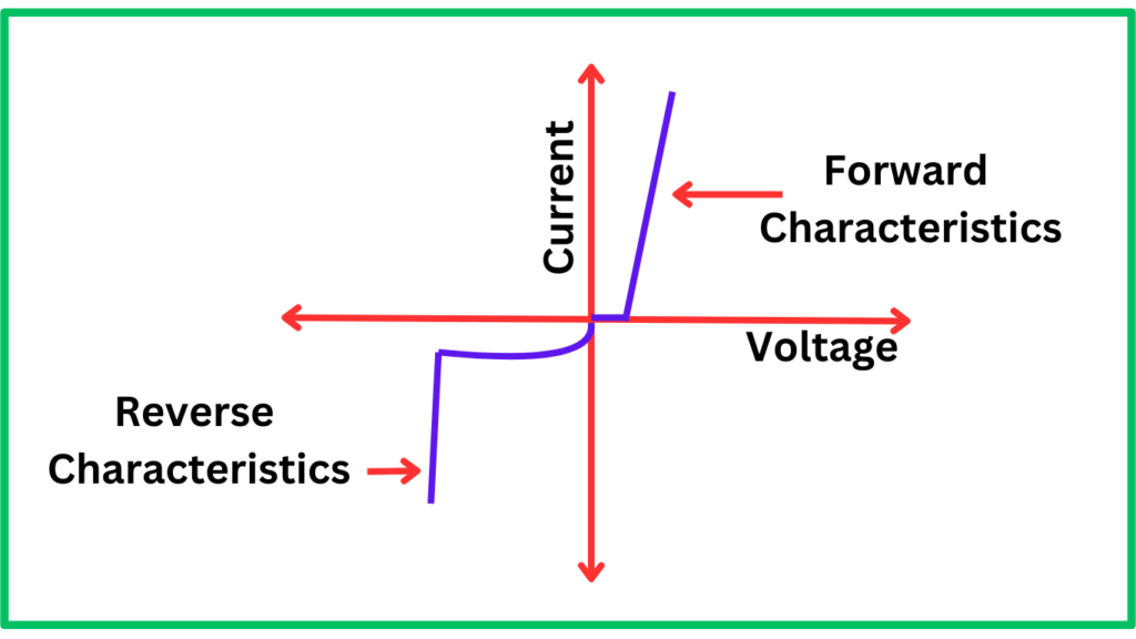
- Forward Bias: When a positive voltage is applied to the metal side relative to the semiconductor, the barrier potential decreases, and electrons easily flow from the semiconductor into the metal. This results in a low forward voltage drop, typically between 0.2V and 0.4V compared to p-n junction diodes (around 0.7V).
- Reverse Bias: In reverse bias, a Schottky diode blocks current flow as the barrier potential increases. A small leakage current may flow due to its metal-semiconductor junction. They have lower reverse leakage currents than regular diodes, although higher than some specialized diodes.
- Breakdown Voltage: Schottky diodes don’t have a clear breakdown voltage like some other diodes. Instead, they go through avalanche breakdown when the reverse voltage becomes too high. At this point, the diode suddenly allows a large reverse current to flow.
- Cut-in Voltage: The cut-in voltage of a Schottky diode is low, typically 0.2–0.3 V, due to its metal-semiconductor junction.
Energy Band Diagram of Schottky Diode
The energy band diagram of a Schottky diode shows the energy levels at the junction of a metal and an n-type semiconductor.
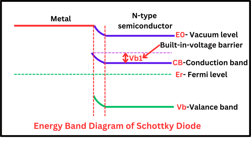
Here’s a detailed explanation of the energy band diagram for a Schottky diode:
Metal Side (Left Side of the Diagram): The metal’s Fermi level is relatively high and located near its conduction band, resulting in a substantial number of free electrons within the metal.
Semiconductor Side (Right Side of the Diagram): The semiconductor, typically n-type silicon in Schottky diodes, features a conduction band (CB), valence band (VB), and a distinct intrinsic energy gap (Eg). Since n-type silicon has many more free electrons, its Fermi level lies closer to the conduction band. and has a higher electron concentration.
Schottky Barrier Formation: When the metal and semiconductor come into contact, their Fermi levels align at equilibrium, causing the bands in the semiconductor near the junction to bend upward. This creates a potential energy difference known as the Schottky barrier height (Vb), which acts as an energy hurdle for electrons moving from the semiconductor into the metal.
Forward Bias Condition: Under forward bias, electrons in the metal gain sufficient energy to cross the Schottky barrier into the semiconductor’s conduction band, resulting in a significant current flow. This process defines the diode’s low forward voltage drop and rapid response time.
Reverse Bias Condition: In reverse bias, the barrier height impedes the flow of electrons from the semiconductor back into the metal.
Schottky Clamped Transistor
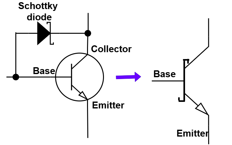
Clamping refers to controlling voltage levels by shifting an input signal to a specific range, achieved by modifying its characteristics.
To create a Schottky-clamped transistor, a Schottky diode is connected in parallel with the transistor’s base-emitter junction. This setup results in a specialized transistor with notable advantages.
One of the key benefits of this design is enhanced switching speed and efficiency. The Schottky diode is strategically positioned to form a low-resistance path for the base current, allowing current to flow with minimal resistance.
Thanks to the diode’s low forward voltage drop and fast switching properties, it clamps the voltage across the base-emitter junction to a lower level than a conventional BJT. This reduces charge storage time, enabling the transistor to turn off more quickly.
Such a design is widely used in applications that demand high-speed switching, such as RF amplifiers and high-performance digital circuits.
Schottky Diodes in Logic Gates
The Schottky diode is widely used in digital circuits, especially in Schottky Transistor-Transistor Logic (TTL) digital logic gates and circuits. These diodes are chosen for their higher frequency response, faster switching times, and lower power consumption. When high-speed switching is needed, Schottky-based TTL is the preferred choice.
There are various versions of Schottky TTL, each offering different speeds and power consumption. The three main TTL logic series using Schottky diodes are:
- Schottky Diode Clamped TTL (S series) – Schottky “S” series (74SXX) is an advanced version of the original diode-transistor DTL. It incorporates Schottky diodes across the base-collector junctions of switching transistors, preventing saturation and reducing propagation delays, leading to faster performance.
- Low-Power Schottky (LS series) – The 74LSXX series offers improved transistor switching speed, stability, and lower power consumption compared to the earlier 74SXX series. This makes it an excellent choice for applications where power efficiency is crucial.
- Advanced Low-Power Schottky (ALS series) – The 74ALSXX series features an even better performance with reduced propagation delay and significantly lower power dissipation. Although more advanced and costly due to its complex internal design, it remains a highly efficient choice for modern digital circuits.
Characteristics of Schottky Diode
The following are the characteristics of the Schottky diode.
- Low forward voltage drop: The Schottky diode has low forward voltage, typically 0.2 to 0.4V. This allows the diode to conduct at low voltage with minimal power loss
- Fast switching speed: Due to the absence of a p-n junction, Schottky diodes have extremely rapid transitions between on and off states. This feature makes them suitable for high-speed switching.
- High efficiency: Schottky diodes offer minimal power loss even at high frequencies, making them highly efficient for applications requiring fast switching and low energy consumption.
- Fast recovery time: Schottky diodes have a fast recovery time.
- Reverse Leakage Current: In terms of reverse bias, Schottky diodes have a higher leakage current than conventional diodes. This is because the metal-semiconductor junction has a lower barrier for minority carriers, resulting in a slight increase in reverse current at higher reverse voltages.
- Reverse Leakage Current at increased temperature: Schottky diodes experience a significant increase in reverse leakage current with rising temperature. As the junction temperature rises by 25°C, the reverse current typically increases by a factor of ten.
- High reverse leakage current: A disadvantage compared to some diodes.
- Low junction capacitance: Ideal for RF and microwave applications.
- High current density: Schottky diodes have a high current density.
Applications of Schottky Diode
Schottky diodes are widely used in various applications due to low forward voltage drop, fast switching speed, and low power consumption. Here are some key applications:
- Power Rectification: Schottky diodes are commonly used in power supply circuits for efficient rectification of high-frequency alternating currents (AC) to direct current (DC), minimizing energy losses.
- High-Frequency Switching: Due to their fast switching capabilities, Schottky diodes are ideal for high-frequency applications in telecommunications, radio frequency (RF) circuits, and data transmission systems.
- Low-Voltage Power Supplies: They are used in low-voltage power supplies where efficiency and minimal power loss are critical, such as in battery-operated devices and portable electronics.
- RF and Microwave Applications: Schottky diodes are commonly employed in RF mixers, modulators, and detectors, offering reliable performance at high frequencies.
- Circuit Protection: In circuit protection applications, Schottky diodes help prevent overvoltage damage by providing quick response to transient events.
- Signal Demodulation: These diodes are used in demodulation circuits, where their rapid switching capabilities help recover signals from modulated carriers.
- Solar Cells: Schottky diodes are used in photovoltaic systems to improve energy efficiency by reducing losses in the diode junction.
- Motor Drives and Inverters: They are utilized in motor drives and inverter circuits to handle high currents and ensure efficient power conversion.
Advantages of Schottky Diode
Schottky diodes offer several advantages that make them suitable for a wide range of applications. Here are the key benefits:
- Low Forward Voltage Drop: Schottky diodes have a much lower forward voltage drop (typically around 0.2 to 0.4 volts) than conventional PN junction diodes, resulting in reduced power loss and higher efficiency.
- Fast Switching Speed: Their metal-semiconductor construction allows for rapid transitions between on and off states, making Schottky diodes ideal for high-speed switching applications, such as in digital circuits and RF systems.
- Low Reverse Leakage Current: Schottky diodes exhibit minimal reverse leakage current, even at high temperatures, ensuring reliable operation with minimal current flow when in reverse bias.
- High Efficiency: Due to their low power loss, Schottky diodes are highly efficient, especially in power rectification and low-voltage applications.
- Thermal Stability: They offer good thermal stability and can operate effectively at elevated temperatures, making them suitable for demanding environmental conditions.
- Reduced Switching Losses: Their fast recovery time minimizes switching losses, which is crucial for applications requiring rapid switching, such as in power inverters and motor drives.
- Compact Size: Schottky diodes are generally smaller in size compared to traditional diodes, allowing for more compact and efficient circuit designs.
- Wide Temperature Range: They can operate effectively over a broad temperature range, making them versatile for various industrial and consumer electronics applications.
Disadvantages of Schottky Diode
While Schottky diodes have many advantages, they also come with some limitations:
- Higher Reverse Leakage Current: Schottky diodes exhibit a higher reverse leakage current compared to conventional PN junction diodes. This can be a concern in applications where minimal leakage is critical, especially at higher temperatures.
- Lower Reverse Breakdown Voltage: They have a lower reverse breakdown voltage, meaning they can handle less voltage in reverse bias without damage. This limits their use in high-voltage applications.
- Temperature Sensitivity: Schottky diodes are more sensitive to temperature variations, as their reverse leakage current increases significantly with rising temperature. This can affect performance in high-temperature environments.
- Higher Cost: Due to the specialized materials and manufacturing processes used in Schottky diodes, they tend to be more expensive than conventional diodes, which may be a factor in cost-sensitive applications.
- Reduced Efficiency at High Reverse Bias: While efficient at low forward voltage drops, Schottky diodes are less efficient when used in high reverse bias conditions, limiting their use in certain power rectification applications.
What is the Difference Between Schottky Diode and PN Junction Diode?
| Feature | Schottky Diode | PN Junction Diode |
|---|---|---|
| Junction Type | Metal-semiconductor | P-N junction |
| Forward Voltage Drop | 0.2 to 0.4V | 0.7V |
| Switching Speed | Faster | Slower |
| Reverse Leakage Current | Higher | Lower |
| Applications | High-speed and low-voltage | General-purpose |
| Reverse Voltage Rating | Lower | Higher |
Frequently Asked Questions – FAQs
1. Why is the forward voltage drop of a Schottky diode lower?
The metal-semiconductor junction allows easier electron flow, reducing energy loss and forward voltage drop.
2. Can Schottky diodes handle high voltages?
No, Schottky diodes are best for low-voltage applications due to their lower reverse voltage rating.
3. Where are Schottky diodes commonly used?
They are used in power supplies, RF circuits, digital logic gates, and voltage clamping applications.
4. What is the Schottky diode symbol?
The Schottky diode symbol features a triangle pointing to a vertical line with a curve, representing the metal-semiconductor junction.
5. How does the working of a Schottky diode differ from a regular diode?
A Schottky diode operates with a metal-semiconductor junction, while a regular diode uses a p-n junction.