Transition and Diffusion Capacitance in PN Junction Diode
Explore transition and diffusion capacitance in PN junction diodes. Understand how transition capacitance (CT) varies with reverse bias and depletion region width, while diffusion capacitance (CD) depends on charge storage in forward bias.
Transition Capacitance
1. Definition: Transition capacitance (CT) is the capacitance that exists in a reverse-biased PN junction due to the variation of charge in the depletion region with applied voltage.
2. Dependence on Reverse Bias: It decreases as the reverse bias voltage increases because the depletion region widens, reducing charge storage.
3. Expression: It is given by the formula:

Where A is the junction area, ε is permittivity, and W is the depletion width.
4. Significance in High-Frequency Circuits: It affects the performance of diodes, particularly in RF and microwave applications, where junction capacitance influences signal transmission.
5. Found in PN Junction Diodes: It is a key parameter in rectifier diodes, varactor diodes, and other semiconductor devices where junction behavior impacts circuit operation.
6. Used in Varactor Diodes: In varactor diodes, transition capacitance is exploited for voltage-controlled tuning applications, such as in radio and TV tuners.
7. Inverse Relation with Voltage: Since depletion width W increases with reverse voltage, transition capacitance follows an inverse power law:
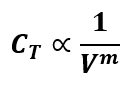
where m depends on the doping profile of the diode.
Diffusion Capacitance
1. Formation in Forward Bias: Diffusion capacitance (CD) arises in a forward-biased PN junction due to the storage of minority charge carriers injected across the junction.
2. Charge Storage Mechanism: In forward bias, electrons diffuse from the N-side to the P-side, and holes diffuse from the P-side to the N-side, leading to an accumulation of charge carriers near the junction. This stored charge contributes to capacitance.
3. Expression for Diffusion Capacitance: It is given by:
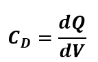
Where Q is the charge stored in the depletion region, and V is the applied voltage. It can also be approximated as:
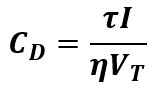
where I is the diode current, τ is the carrier lifetime, and VT is the thermal voltage.
4. Dependence on Forward Current: Diffusion capacitance is directly proportional to the diode current (I), making it significant in forward-biased conditions. It increases with increasing forward bias.
5. Much Larger Than Transition Capacitance: In forward bias, diffusion capacitance is typically much larger than transition capacitance, sometimes exceeding it by several orders of magnitude.
6. Impact on High-Speed Switching: High diffusion capacitance in forward-biased diodes can slow down switching speeds in electronic circuits, especially in rectifiers and signal processing applications.
7. Application in High-Frequency Circuits: Diffusion capacitance plays a crucial role in determining the response time of diodes in fast-switching applications, such as in RF circuits and digital electronics.