Question:
Which of the Following Defines an N-type semiconductor?
- A semiconductor with excess of black holes is called N-type
- A semiconductor with an excess of electrons is called N-type
- A semiconductor with an excess of holes is called N-type
- A semiconductor with an excess of electrons and holes is called N-type
Answer:
The correct option is (2).
Which of the Following Defines an N-type semiconductor? Answer: A semiconductor with an excess of electrons is called an N-type semiconductor. Why does an N-type semiconductor have excess electrons?” Here is an explanation to help clarify this concept.
Explanation:
In semiconductors, the distinction between n-type and p-type materials comes from the types of impurities added to the intrinsic (pure) semiconductor, which alter its electrical properties. An n-type semiconductor is created by doping an intrinsic semiconductor with donor impurities that have more valence electrons than the semiconductor itself.
Here’s a step-by-step explanation of why n-type semiconductors have excess electrons:
1. Intrinsic Semiconductor Composition
An intrinsic semiconductor, typically silicon or germanium, has a crystalline structure where each atom shares electrons with its neighbors through covalent bonds. Silicon and germanium both have four valence electrons, which means they can form stable structures by sharing electrons in a tetrahedral lattice.
2. Doping with Donor Impurities
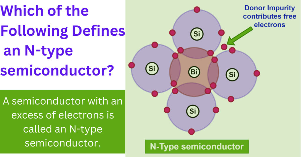
To create an n-type semiconductor, the pure semiconductor is doped with atoms that have more than four valence electrons—typically five. Common donor atoms for silicon include phosphorus or arsenic.
3. Energy Levels and Electron Donation
In a silicon crystal, silicon atoms are replaced by these donor atoms. While the four of the donor’s five electrons are used to maintain the structural integrity of the crystal by bonding with adjacent silicon atoms, the fifth electron is not required for bonding and is comparatively loosely bound to the donor atom.
4. Conduction Band and Extra Electrons
The energy required to free this extra loosely bound electron is much smaller than the energy needed to break an electron free from a silicon atom. As a result, at room temperature, these extra electrons from the donor atoms gain enough energy to escape from the atomic bond and move freely through the material. These free electrons increase the electron concentration in the semiconductor.
5. Creation of the n-Type Behavior
With these additional free electrons available, the semiconductor exhibits an excess of negative charge carriers (electrons). This excess of electrons gives the material its characteristic n-type behavior, where “n” stands for negative.
6. Electrical Conductivity
Because electrons are mobile charge carriers and there are more of them than holes (which are the absence of electrons and act as positive charge carriers in semiconductors), the electrical conductivity of the semiconductor is largely due to the motion of these electrons. Thus, n-type semiconductors are efficient in conducting electricity due to the abundance of free electrons.
In summary, n-type semiconductors have excess electrons because they are doped with atoms that contribute extra electrons that are not tied up in bond formation and readily contribute to electrical conductivity.
Thus, excess electrons defines that the material is an N-type semiconductor.
Q1. The Forbidden Energy Gap for Germanium is:
Q2. What is the forbidden energy gap in a pure conductor?
Q3. Leakage Current in the Silicon Semiconductor is in the order of