Discover the key diode characteristics, including forward and reverse bias behavior, breakdown voltage, knee voltage, peak inverse voltage, and more. Learn how these properties impact diode performance in electronic circuits.
There are different current levels in forward bias and reverse bias operations. In the forward bias region, the diode allows current to flow easily. This happens when the P-region is made positive, and the N-region is made negative.
The diode allows almost no current to flow in the high-resistance direction. This happens when the P-region is negative and the N-region is positive. In this condition, holes and electrons move away from the junction. As a result, the barrier potential increases. This effect is shown in the reverse current portion of the curve.
The dotted section of the curve represents the ideal diode behavior. This ideal curve would exist if there were no avalanche breakdowns. The following figure shows the static characteristics of a junction diode.

Diode IV Characteristics
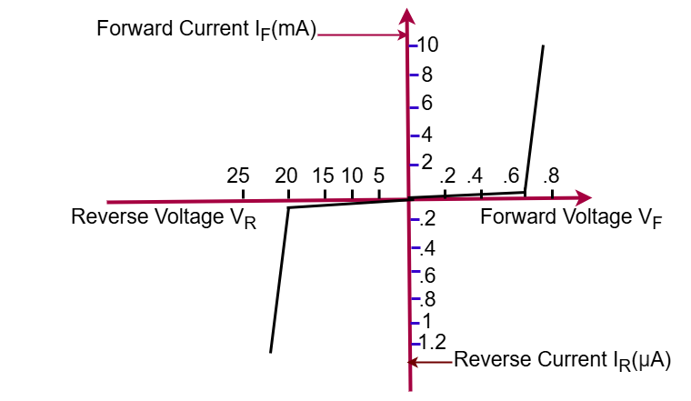
The IV characteristics of a diode for forward and reverse bias are typically shown on a single graph. The figure in the Forward Characteristic section represents this relationship. Forward Voltage (VF) and Reverse Voltage (VR) are plotted along the horizontal axis in the graph.
The forward and reverse current values are shown on the vertical axis of the graph. Forward Voltage (VF) is plotted to the right, while Reverse Voltage (VR) is plotted to the left. The zero point is located at the center of the graph. Forward Current (IF) increases above the horizontal axis, while Reverse Current (IR) extends downward.
The Forward Voltage (VF) and Forward Current (IF) appear in the upper right section of the graph. The Reverse Voltage (VR) and Reverse Current (IR) are shown in the lower left section. Typically, different scales are used to display forward and reverse values for better clarity.
Forward Characteristics of Diode
When a diode is forward-biased, it allows current to flow in the forward direction. The forward current (IF) depends directly on the applied forward voltage (VF). The relationship between the forward voltage (VF) and forward current (IF) is known as the ampere-volt (IV) characteristic of a diode. This characteristic provides a clear understanding of how a diode behaves when a voltage is applied in the forward direction.
A typical diode forward IV characteristic is shown in the figure below.
The following observations can be made:
- Initial Condition (VF = 0V, IF = 0 mA)
- When no external voltage is applied across the diode terminals (VF = 0V), no current flows through it (IF = 0 mA).
- This is because the potential barrier at the P-N junction prevents the movement of charge carriers.
- Gradual Increase in Forward Voltage (VF)
- As the forward voltage VF is increased in small steps (e.g., 0.1V increments), the forward current IF begins to increase gradually.
- Initially, this increase is very small due to the presence of the depletion region, which still acts as a barrier to charge carriers.
- Knee Voltage (VK) – Breakdown of Barrier Potential
- When VF reaches a certain threshold value, known as the knee voltage (VK), the potential barrier at the P-N junction is overcome.
- At this point, the forward current (IF) increases rapidly.
- The knee voltage values for different diodes are:
- Silicon Diodes: VK ≈ 0.7V
- Germanium Diodes: VK ≈ 0.3V
- Beyond this point, a slight increase in VF results in a large increase in IF.
- Excessive Forward Current and Heat Generation
- If VF is further increased beyond VK, the forward current (IF) rises exponentially.
- This operation leads to excessive heat generation within the diode junction, which can damage or destroy the diode.
- This effect is more severe if the diode is not current-limited by an external component.
A series resistor is connected to the circuit to protect the diode from excessive current. This resistor limits forward current IF and prevents the diode from overheating and burning out. The value of the resistor is chosen based on the maximum rated current of the diode.
Reverse Characteristics of Diode
When a diode is reverse-biased, it resists the flow of current. The Reverse Voltage (VR) is applied by making the P-region negative and the N-region positive. This prevents charge carriers from moving across the junction, creating a high-resistance state.
Observations on Reverse Characteristics
- Initial Condition (VR = 0V, IR = 0 mA)
- When no external voltage is applied (VR = 0V), no reverse current (IR) flows through the diode.
- The depletion region remains intact, preventing carrier movement.
- Small Leakage Current in Reverse Bias
- As the Reverse Voltage (VR) increases, a small leakage current appears due to minority charge carriers.
- This current is very small (in microamperes for silicon diodes) and is almost constant with increasing VR.
- Breakdown Region – Avalanche Breakdown or Zener Breakdown
- When VR reaches a certain breakdown voltage (VBR), the reverse current (IR) increases rapidly.
- This happens due to either avalanche breakdown (in regular diodes) or Zener breakdown (in Zener diodes).
- At this point, the diode loses its ability to block current, allowing a sudden large reverse current to flow.
- Destruction Risk in Breakdown Region
- If the reverse current becomes too large, it can overheat and damage the diode.
- Special diodes like Zener diodes are designed to operate safely in the breakdown region.
Graphical Representation
- The Reverse Voltage (VR) is plotted on the left side of the graph.
- The Reverse Current (IR) extends below the horizontal axis.
- The zero point is at the center of the graph.
- The reverse characteristic curve remains flat until it reaches the breakdown region, where it sharply rises.
Diode Specifications
Choosing the right diode for an application is important. Manufacturers provide specifications to help with selection. These include voltage and current ratings, operating conditions, mechanical details, lead identification, and mounting instructions.
Below are some key diode specifications:
- Maximum Forward Current (IFM) – The highest continuous forward current a diode can handle without damage.
- Maximum Reverse Voltage (VRM) – The highest reverse voltage a diode can withstand before breaking down.
- Reverse Breakdown Voltage (VBR) – The minimum reverse voltage at which the diode enters breakdown and starts conducting significantly.
- Maximum Forward Surge Current (IFM-surge) – The maximum short-duration forward current the diode can tolerate. This is much higher than the continuous forward current limit.
- Maximum Reverse Current (IR) – The highest reverse leakage current the diode can withstand at its rated operating temperature.
- Forward Voltage (VF) – The voltage drop across the diode when conducting a specific forward current.
- Power Dissipation (PD) – The maximum power the diode can safely handle continuously in free air at 25°C.
- Reverse Recovery Time (Trr) – The time required for the diode to switch from conducting to non-conducting mode.
Important Terms
- Breakdown Voltage (VBR) – The minimum reverse voltage at which the PN junction breaks down and allows a sudden rise in reverse current. Beyond this voltage, the diode can get damaged if not properly limited.
- Knee Voltage (VK) – The forward voltage at which the current through the junction starts increasing rapidly. This marks the transition from a low conduction state to a high conduction state. It is approximately 0.3V for germanium diodes and 0.7V for silicon diodes.
- Peak Inverse Voltage (PIV) – The maximum reverse voltage that can be applied to a diode without causing damage. If exceeded, it may lead to junction breakdown.
- Maximum Forward Current Rating (IFM) – The highest forward current a diode can safely conduct without overheating or failure. Exceeding this limit can damage the diode.
- Maximum Power Dissipation (PD) – The maximum power that the diode can handle continuously without exceeding safe temperature limits. It is usually specified at 25°C in free air.
- Reverse Recovery Time (Trr) – The time taken by a diode to switch from conducting (forward-biased) to non-conducting (reverse-biased) mode. This is important in high-speed switching applications.
- Junction Capacitance (Cj) – The capacitance formed by the depletion layer of the diode, which affects high-frequency performance.
Read Next: