An op-amp comparator is an open-loop circuit that evaluates an input voltage against a reference level and generates a binary output according to which voltage is greater.
What is an Op-Amp Comparator?
An op-amp comparator is an electronic circuit that compares one analogue input voltage with another input voltage or a predetermined reference voltage, . It produces an output signal based on the relative levels of the two voltages.
In simple terms, an op-amp voltage comparator determines which of the two input voltages has the higher magnitude and changes its output accordingly.
The output voltage formula of an op-amp is:
where is the voltage applied to the non-inverting terminal, is the voltage applied to the inverting terminal, and represents the open-loop voltage gain of the op-amp.
How an Op-amp Comparator Works
Voltage comparators generally operate either with positive feedback or without feedback, in an open-loop configuration, to switch the output between two saturation levels. In open-loop operation, the op-amp retains its very high open-loop voltage gain, .
Because of this high gain, even a small difference between the input voltages can drive the comparator output toward either the positive supply rail, , or the negative supply rail, , when the input crosses a preset threshold voltage.
An open-loop op-amp comparator operates in the non-linear region. Changes in the two input voltages, and , cause the output to switch between two distinct states, and . In this respect, it behaves similarly to a digital bistable device.
Therefore, a voltage comparator can be viewed as a 1-bit analogue-to-digital converter, because it accepts an analogue input but produces an output with two distinct digital-like states.
The basic op-amp voltage comparator circuit is shown below.
Op-amp Comparator Circuit Diagram
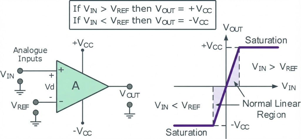
With reference to the op-amp comparator circuit shown above, let us first consider the condition where the input voltage is lower than the reference voltage
Therefore, since the voltage at the non-inverting (+) input is lower than the voltage at the inverting (−) input, the comparator output switches LOW, approaching the negative supply voltage, . This drives the output into negative saturation.
As the input voltage is increased above the reference voltage at the inverting input, the comparator output quickly switches HIGH, approaching the positive supply voltage, . This drives the output into positive saturation.
If is then reduced below , the output switches back to the negative saturation level, . In this way, the op-amp comparator operates as a threshold detector, changing its output state whenever the input crosses the reference voltage.
Op-Amp Comparator Output States and Logic Levels
An op-amp voltage comparator can be considered a binary device because its output switches between HIGH and LOW depending on the input voltage relative to a fixed DC reference voltage.
The comparator output becomes HIGH when the voltage at the non-inverting input is higher than that at the inverting input, and switches LOW when the non-inverting input voltage falls below the inverting input voltage. This behavior remains the same regardless of whether the input signal is applied to the inverting or non-inverting terminal.
The output voltage is also determined by the op-amp’s power supply voltage. In theory, its extremely high open-loop gain could produce an infinitely large output voltage in either direction, represented as .
In practice, however, the output cannot exceed the available supply rails and therefore is limited to approximately:
As discussed earlier, a basic op-amp comparator generates a positive or negative output by comparing the input voltage with a predetermined DC reference level.
A resistive voltage divider is commonly used to establish the comparator’s reference voltage. Alternatively, a battery, Zener diode, or potentiometer can be used when a fixed or adjustable reference voltage is required.
How to Generate Comparator Reference Voltages
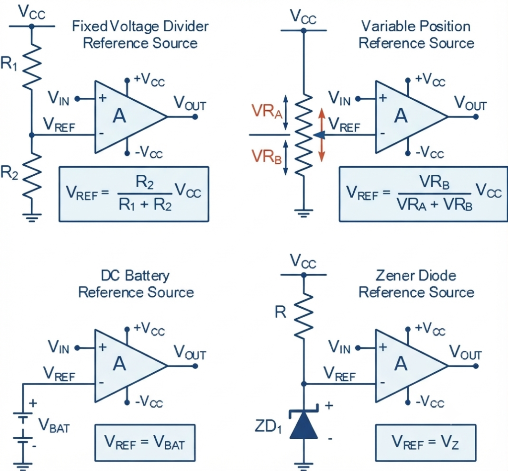
In theory, the comparator reference voltage can be set anywhere from up to the supply voltage. However, the practical reference-voltage range is limited by the specific op-amp comparator device being used.
Positive and Negative Voltage Comparators
A basic op-amp comparator can detect either positive-going or negative-going input signals, depending on how the input voltage and fixed reference voltage are connected to the op-amp terminals.
In the circuits discussed above, the fixed reference voltage is applied to the inverting input, while the input signal is connected to the non-inverting input.
The connections can also be reversed. Doing so changes the polarity of the comparator output relative to the input signal. Based on the arrangement of the input and reference connections, the op-amp comparator can operate in either an inverting or non-inverting configuration.
The Positive Voltage Comparator
A positive voltage comparator, also known as a non-inverting comparator, detects when the input voltage rises above the reference voltage . When , the comparator output switches HIGH.
Non-inverting Comparator Circuit
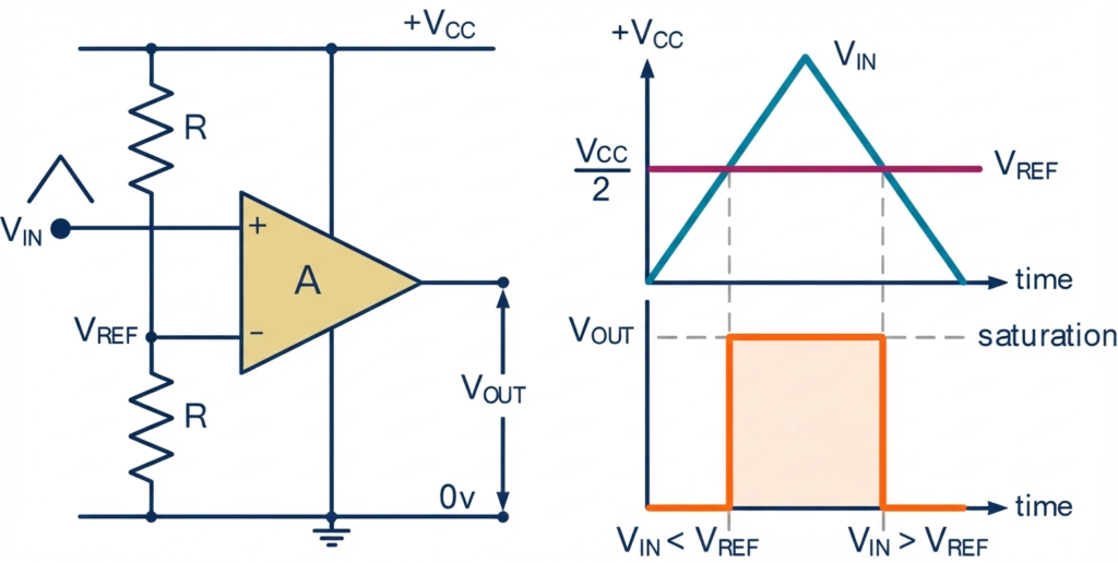
In this non-inverting comparator configuration, the reference voltage is applied to the op-amp’s inverting input, while the input signal is connected to the non-inverting input.
For simplicity, assume that the two resistors in the voltage-divider network are equal:
This arrangement sets the reference voltage to half of the supply voltage:
while can vary from to .
When , the comparator output switches HIGH and saturates toward the positive supply rail, . When , the output changes state and saturates toward the negative supply rail.
The Negative Voltage Comparator
A negative voltage comparator, also known as an inverting comparator, detects when the input voltage falls below or becomes more negative than the reference voltage . Under this condition, the comparator output switches HIGH, as shown.
Inverting Comparator Circuit
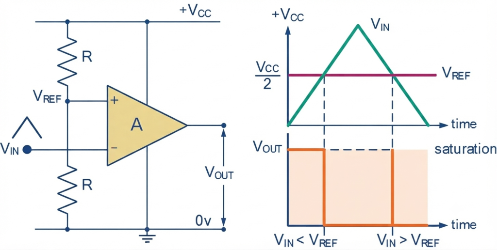
In an inverting comparator configuration, the input connections are reversed compared with the non-inverting arrangement. The reference voltage is applied to the non-inverting input, while the input signal is connected to the inverting input.
When , the comparator output switches HIGH and saturates toward the positive supply rail, . Conversely, when , the output changes state and saturates toward the negative supply rail, .
Thus, selecting different op-amp terminals for the input signal and reference voltage determines whether the comparator produces an inverting or non-inverting output.
This concept can be extended further by combining the two comparator configurations to detect whether an input voltage lies within a specified range, forming a window comparator circuit.
Window Comparator
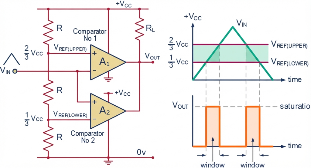
A Window Comparator Circuit combines the inverting and non-inverting comparator configurations to determine whether an input voltage falls within a specified range, or voltage window. Unlike a basic comparator, which indicates whether the input is above or below a single reference level, a window comparator uses two reference voltages to define an acceptable voltage range.
The two reference levels are established using a pair of voltage comparators. The upper threshold is represented by , while the lower threshold is represented by .
The range between these upper and lower reference voltages is known as the window, which gives the circuit its name.
A simple window comparator can be constructed using three equal-value resistors:
Since the resistors have equal values, the supply voltage is divided into three equal voltage intervals. Each resistor therefore has a voltage drop of:
For this example, the upper reference voltage can be set to:
and the lower reference voltage to:
Thus, the input voltage range between and forms the window. The basic window comparator circuit is shown below.
Window Comparator Circuit
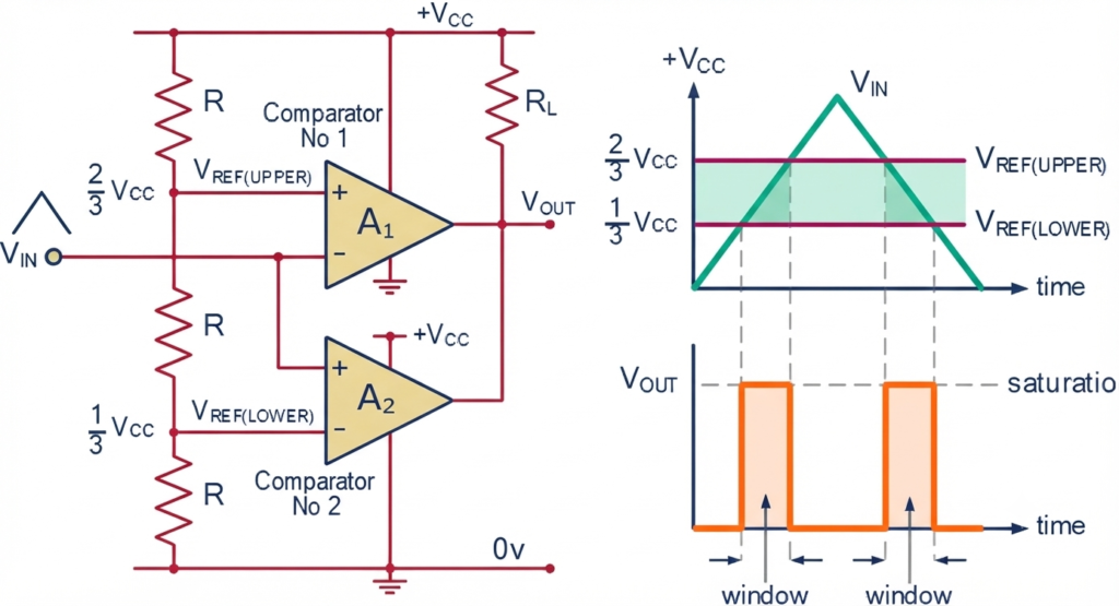
The circuit initially operates with the open-collector output of op-amp A1 OFF, while the output of op-amp A2 is ON and sinking current. Under this condition, the output voltage is .
When is below the lower reference level,
the output remains LOW. As rises above this lower threshold, the first comparator detects the change and switches its open-collector output HIGH.
At this point, both comparator outputs are HIGH, so no current flows through the pull-up resistor . Consequently, the output voltage rises to the supply voltage:
As continues to increase and exceeds the upper reference level,
the second comparator switches its output LOW. This pulls the circuit output down, making:
Thus, the window comparator produces a HIGH output only when the input voltage lies between the lower and upper reference levels.
Defining the Comparator Window
The difference between and defines the switching window for a positive-going input signal. In this example:
Now assume that is initially at its maximum value, equal to . As decreases and crosses the upper reference level , the second comparator switches its output HIGH.
As continues to fall and passes below the lower reference level , the first comparator switches the output LOW again. Therefore, the difference between the two reference levels also defines the switching window for a negative-going input signal.
consequently changes between HIGH and LOW as moves above or below the upper and lower reference thresholds.
In this simple example, the upper and lower trip levels are set to and , respectively, because three equal-value resistors are used. However, the reference levels can be adjusted to suit a particular application, allowing the window width to be customized.
If a dual power supply is used and the upper and lower trip levels are set to and , respectively, a sinusoidal can be applied. The window comparator can then function as a zero-crossing detector, producing a HIGH or LOW output whenever the sine wave crosses the zero-voltage level in either direction.
The concept can be extended further by connecting several op-amp comparators to a common input signal, while assigning each comparator a different reference voltage through a voltage-divider network. This arrangement forms a voltage level detector circuit.
Comparator Voltage Level Detector
A voltage level detector uses multiple op-amp comparator circuits, with each comparator assigned a different reference voltage. A common voltage-divider network provides these reference levels to comparators A1 through A4. With equal-value resistors, five resistors are required to generate four different reference voltages.
The voltage at the junction of the bottom pair of resistors is:
The successive reference levels are:
with the final level reaching:
As the common input voltage increases, the comparator outputs change state one after another. The connected LEDs switch OFF sequentially, beginning with the lower comparator A4 and progressing upward toward A1 as the input voltage rises.
By selecting appropriate resistor values in the voltage-divider network, the comparator thresholds can be set to detect specific voltage levels. One practical application is a battery condition monitor, where the LEDs can be reversed and connected to (ground) instead of to indicate different battery voltage conditions.
The number of detection levels can also be increased by adding more op-amp comparators. For example, eight comparators can provide eight trigger levels. If their outputs are connected to an 8-to-3 line digital encoder, the arrangement can form a simple analogue-to-digital converter (ADC) that converts the analogue input into a 3-bit binary code ranging from 0 to 7.
Op-Amp Comparator with Positive Feedback
An operational amplifier can be used as a comparator by operating it in open-loop mode. This arrangement works well when the input signal changes quickly and remains relatively free from noise. However, problems can occur when the input voltage changes slowly or contains electrical noise.
When the input voltage,, approaches the reference voltage, , even a small amount of noise can cause the comparator output to switch repeatedly between its two saturation levels, and . This rapid and unwanted switching is often referred to as chattering or oscillation around the switching point.
A common way to eliminate this problem is to introduce positive feedback into the comparator circuit. Positive feedback feeds a portion of the output voltage back to the non-inverting input of the op-amp. The feedback voltage is usually obtained using a resistor divider, with the amount of feedback determined by the values and ratio of the two resistors.
Positive feedback changes the switching behavior of the comparator. Once the output reaches one of its saturation levels, the feedback shifts the effective switching threshold. As a result, the input voltage must change by a definite amount before the output can switch to the opposite saturation state.
This creates two different switching threshold voltages rather than a single switching point. The voltage difference between these two thresholds is known as hysteresis.
The addition of positive feedback therefore makes the comparator much less sensitive to noise and prevents unwanted output transitions when the input signal is close to the switching level. A comparator designed with this type of hysteresis is commonly known as a Schmitt trigger.
The operation can be understood using the inverting comparator with positive feedback shown below.
Inverting Op-Amp Comparator with Hysteresis
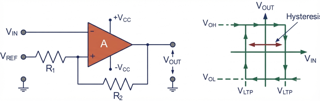
In the inverting op-amp comparator with hysteresis, the input voltage is connected to the inverting (−)(-) terminal of the op-amp. Resistors and form a voltage-divider network that provides positive feedback from the output to the non-inverting terminal.
A portion of the output voltage is fed back to the non-inverting input through this resistor network. The amount of feedback depends on the relative values of and . Therefore, changing the resistor ratio changes the feedback voltage and, consequently, the switching thresholds of the comparator.
Voltage Divider Equation for Beta
The resistor network used for positive feedback determines what fraction of the comparator output is returned to the non-inverting input. This fraction is represented by the Greek letter β\beta and is called the feedback factor or feedback fraction.
For the voltage-divider network:
Therefore, the feedback voltage applied to the non-inverting input is:
where:
- = feedback fraction
- = comparator output voltage
- = voltage appearing at the non-inverting input
The operation of the comparator can now be understood by considering the two possible output states.
When the Output is HIGH
When the input voltage is below the reference level, , the comparator output remains HIGH. Assuming the output has reached its positive saturation level, the voltage fed back to the non-inverting input is approximately:
This positive reference level is called the Upper Trip Point (UTP):
As increases, it eventually reaches the upper trip point. At this level, the comparator changes state and its output switches from positive saturation to negative saturation.
When the Output is LOW
After the output switches LOW, the polarity of the feedback voltage also reverses. The non-inverting input now receives a negative reference voltage:
This voltage is known as the Lower Trip Point (LTP):
The output will remain in the LOW state until decreases below this lower trip point. Once this occurs, the comparator switches back to its positive saturation state.
Upper and Lower Trip Points
The important feature of positive feedback is that the comparator no longer has a single switching threshold. Instead, the feedback network creates two separate switching levels:
- Upper Trip Point (UTP): the input voltage at which the output switches from HIGH to LOW.
- Lower Trip Point (LTP): the input voltage at which the output switches from LOW to HIGH.
The voltage difference between these two levels is called hysteresis.
For a symmetrical comparator with output saturation levels of and :
and
Therefore, the total hysteresis voltage is:
The value of hysteresis depends directly on the feedback factor . A larger feedback fraction produces a wider hysteresis band.
This hysteresis makes the comparator much less sensitive to small voltage fluctuations and electrical noise around the switching threshold. The input voltage must cross the appropriate trip point before the output changes state, preventing repeated or erratic switching when the input changes slowly or contains noise. This is the key operating principle behind the Schmitt trigger.
Op-Amp Comparator Hysteresis
A comparator with hysteresis can also be configured in a non-inverting arrangement. In this configuration, the positions of the input and reference connections are interchanged compared with the inverting hysteresis comparator.
The input voltage is applied to the non-inverting (+) terminal, while the positive-feedback network is connected to the inverting (−) terminal. The resistor network feeds a portion of the output voltage back to the inverting input, establishing two distinct switching thresholds.
As a result, the comparator does not respond to small fluctuations around a single reference voltage. Instead, the input must cross one of the two threshold levels before the output changes state. The difference between these thresholds forms the hysteresis band, which improves switching stability and helps prevent unwanted output transitions caused by noise or slowly varying input signals.
Non-Inverting Op-Amp Comparator with Hysteresis
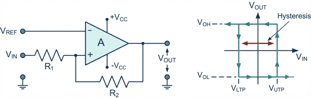
A non-inverting op-amp comparator with hysteresis uses positive feedback to create two distinct switching thresholds. The input voltage is applied to the non-inverting terminal, while the feedback network establishes the reference level at the inverting terminal.
Because the reference level changes with the output state, the comparator switches at different input voltages depending on whether the input is increasing or decreasing. This difference between the two switching levels produces the hysteresis band.
The hysteresis graph illustrates this behavior clearly. The arrows indicate the direction in which the output changes as the input voltage moves through the two trip points:
- At the Upper Trip Point (UTP), an increasing input voltage causes the comparator output to switch from LOW to HIGH.
- At the Lower Trip Point (LTP), a decreasing input voltage causes the output to switch from HIGH to LOW.
Between the UTP and LTP, the output retains its previous state. Therefore, small fluctuations or noise within this voltage range do not cause unwanted switching.
This characteristic makes the non-inverting hysteresis comparator useful for converting slowly varying or noisy input signals into a stable, we
Op-Amp Comparator Worked Example
A operational amplifier is configured with positive feedback to operate as a Schmitt trigger. The feedback network consists of two resistors, and .
Determine the upper switching threshold, lower switching threshold, and hysteresis width when the circuit is powered from a dual supply of .
Given:
The supply voltages are:
Step 1: Calculate the Feedback Factor
The feedback factor is:
Substituting the resistor values:
Therefore:
Step 2: Calculate the Upper Switching Point
When the comparator output is at positive saturation, the reference voltage at the input is:
Therefore:
Step 3: Calculate the Lower Switching Point
When the output switches to negative saturation, the feedback voltage reverses polarity:
Thus:
Step 4: Calculate the Hysteresis Width
The hysteresis voltage is the difference between the upper and lower switching points:
Therefore, the upper switching point is +1.8 V, the lower switching point is −1.8 V, and the resulting hysteresis width is 3.6 V.
Voltage Op-Amp Comparator
Although an operational amplifier such as the 741 can be configured to perform voltage comparison, it is not specifically designed for this purpose. A conventional op-amp is primarily optimized for linear amplification, where negative feedback keeps the input terminals at nearly the same voltage and the output operates within its linear range.
When an op-amp is used as a comparator without negative feedback, its very high open-loop gain quickly drives the output toward one of its saturation limits. Furthermore, standard op-amps are generally intended for closed-loop applications, where negative feedback from the output to the inverting input controls the overall gain and maintains stable linear operation.
A dedicated voltage comparator, in contrast, is specifically designed for switching applications. It is a non-linear device intended to respond rapidly when the voltage at one input becomes slightly higher or lower than the voltage at the other input.
Because of its very high gain, even a small difference between the input voltages can force the comparator output rapidly toward one of its two output states. This makes dedicated voltage comparators more suitable than general-purpose op-amps for applications such as zero-crossing detection, level detection, threshold switching, waveform shaping, and Schmitt trigger circuits.
The main difference is therefore that an op-amp is primarily designed to provide controlled linear amplification, whereas a voltage comparator is designed to provide fast and reliable switching between output states.
Op-Amp Comparator vs Voltage Comparator
The primary difference between a general-purpose op-amp used as a comparator and a dedicated voltage comparator lies in the way their output stages are designed.
A standard operational amplifier is primarily intended for linear amplification. Its output stage is optimized to produce a continuously varying output voltage within its operating range. Although an op-amp can be driven into saturation when used as a comparator, this is not its intended operating mode.
A dedicated voltage comparator, on the other hand, is specifically designed for high-speed switching. Its output stage is optimized to operate between two defined states rather than provide a continuously varying analog output. When the input voltage crosses the reference level, the comparator rapidly changes its output state.
Common dedicated voltage comparator ICs include the LM311 single comparator, LM339 quad comparator, and LM393 dual comparator. These devices are available in standard integrated-circuit packages and can be designed to operate from either single or dual power supplies, depending on the device.
Dedicated comparators are designed to switch quickly between their output states. Their output circuitry commonly uses transistor switching stages, allowing the device to respond rapidly when the relationship between the two input voltages changes.
Because a voltage comparator effectively converts an analog input condition into a digital-like output state, it is widely used for applications such as voltage-level detection, zero-crossing detection, threshold detection, waveform conversion, and interface circuits.
Another important distinction is the output configuration. Many comparator ICs, such as the LM393 and LM339, use an open-collector output. Similar devices may use an open-drain configuration. In these arrangements, the output transistor acts primarily as a switch, pulling the output node toward one state when conducting and releasing it when turned off. An external pull-up resistor is typically required to establish the HIGH output level.
Thus, while both an op-amp and a voltage comparator can compare two input voltages, a dedicated comparator is specifically engineered for fast and reliable switching, whereas a conventional op-amp is primarily designed for linear amplification.
Voltage Comparator Circuit
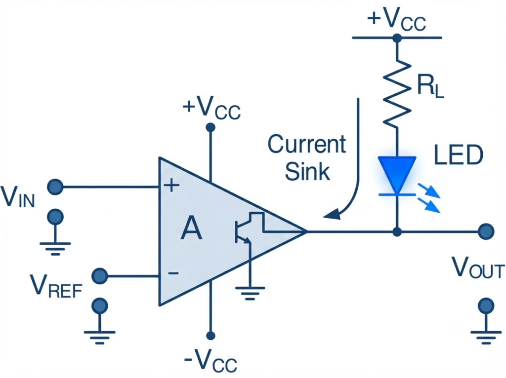
A dedicated voltage comparator with an open-collector output requires an external pull-up resistor to establish a defined HIGH output level. In the circuit shown above, the pull-up resistor is connected between the comparator output and the positive supply voltage. An LED is also included as a visual indicator of the comparator’s switching state.
When the comparator output transistor is OFF, the output presents a high-impedance path to ground. The pull-up resistor then raises the output voltage toward the positive supply:
Since the output transistor is not conducting, little or no current flows through the output transistor.
When the comparator switches ON, its output transistor provides a low-impedance path to ground. Current then flows from the supply through the pull-up resistor and LED and into the output transistor. The voltage across the pull-up resistor and LED causes the output voltage to fall close to ground:
The output therefore behaves essentially as a switch, alternating between a high-impedance OFF state and a low-impedance ON state.
At the circuit level, the basic symbols and input arrangements of an op-amp used as a comparator and a dedicated voltage comparator may appear quite similar. The important distinction is primarily in their output-stage design and intended operating mode.
The open-collector or open-drain output of a dedicated comparator also provides useful flexibility. It can interface with other logic circuits and, with appropriate external circuitry, can be used to control devices such as LEDs, relays, lamps, and transistor switching stages. When a higher load current is required, the comparator output can drive an external power transistor, which provides substantially greater current-handling capability than the comparator output stage itself.
Conclusion
In this article, we have explored how an op-amp comparator works and how an operational amplifier can be used as a voltage-comparison circuit. In its basic form, the op-amp operates in open-loop mode, without negative feedback. When the input voltage crosses the reference voltage, the very high open-loop gain drives the output rapidly toward one of its saturation levels.
The comparator therefore produces two distinct output states depending on the relative voltages at its inverting and non-inverting inputs. This non-linear switching behavior forms the basic operating principle of op-amp comparator circuits.
We also examined the effect of positive feedback. Feeding a portion of the output back to the input creates two separate switching thresholds: the Upper Trip Point (UTP) and Lower Trip Point (LTP). The difference between these thresholds is called hysteresis. This arrangement, commonly known as a Schmitt trigger, prevents unwanted or repeated switching when the input signal changes slowly or contains electrical noise.
A window comparator extends this principle by using two comparator stages and two reference voltages. It can determine whether an input voltage lies above, below, or within a specified voltage range, making it useful for voltage monitoring and level-detection applications.
The tutorial also highlighted the important differences between a conventional operational amplifier and a dedicated voltage comparator. Although an op-amp can be used as a comparator, its internal circuitry is primarily optimized for linear amplification. Dedicated comparator ICs are specifically designed for fast switching and can operate reliably in saturation.
Common devices such as the LM311, LM393, and LM339 are examples of dedicated voltage comparators. Their switching-oriented output stages make them well suited for applications such as voltage-level detection, zero-crossing detection, waveform conversion, interface circuits, and analog-to-digital signal conditioning.
In summary, an op-amp can perform the basic function of a comparator, but a dedicated voltage comparator is generally more appropriate when fast, stable, and reliable switching is required. Understanding open-loop operation, positive feedback, hysteresis, trip points, and comparator output stages provides the foundation for designing and applying comparator circuits effectively.
Read Next:
- Inverting vs Non-Inverting Amplifier: Differences, Gain, and Applications
- Inverting Operational Amplifier: Circuit, Working, and Gain Formula
- Op-Amp Building Blocks: Basic Circuits and Applications
- Operational Amplifier (Op-Amp): Basics, Types, Working & Applications
- Non-inverting Operational Amplifier: Circuit, Gain & Formula
- Summing Amplifier: Circuit, Gain Formula, Derivation & Applications
- Differential Amplifier: Circuit, Types, Formula & Applications
- Op-Amp Integrator Amplifier: Formula, Working & Applications
- Op-Amp Differentiator Amplifier: Circuit, Working, Formula & Applications
- Op-Amp Multivibrator: Working, Circuit, Types & Applications
- Op-Amp Monostable Multivibrator: Circuit, Working, Formula & Timing
- Passive Averager: Circuit, Equation & Op-Amp Averager