The Op-Amp Integrator Amplifier is an important analog circuit used in signal processing and waveform generation. It provides a useful way to process time-varying input signals and forms the basis of several practical op-amp applications.
What Is an Op-Amp Integrator Amplifier?
An Op-Amp Integrator Amplifier is an analog circuit that uses an operational amplifier and a capacitor to perform mathematical integration. It produces an output voltage related to the accumulated value of the input signal over time. This makes the circuit useful for processing time-varying signals and generating different waveforms.
Op-amp integrators find applications in analog computers, analog-to-digital converters (ADCs), signal processing, and wave-shaping circuits. For example, an integrator can convert a square-wave input into a triangular-wave output and a sine-wave input into a cosine-type waveform.
Op-amp Integrator Amplifier Circuit
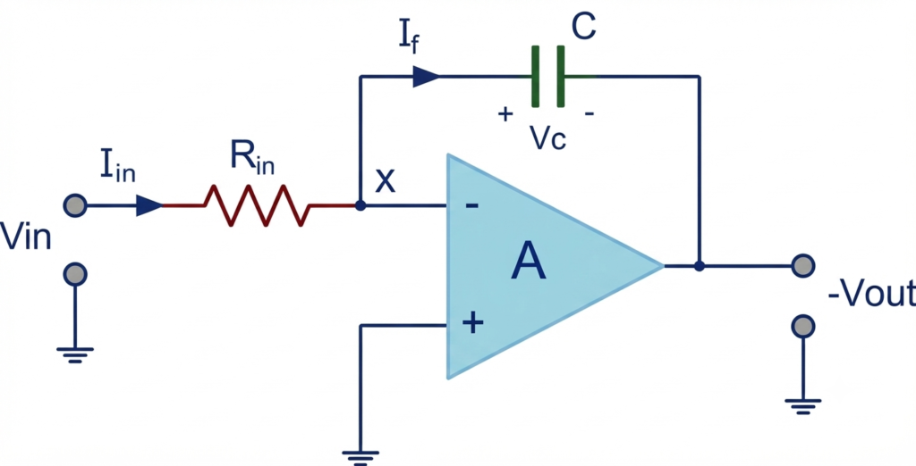
The Op-Amp Integrator Amplifier uses an operational amplifier, an input resistor , and a feedback capacitor . The input voltage is applied to the inverting terminal of the op-amp through , while the non-inverting terminal is connected to ground.
The capacitor provides the feedback path between the op-amp output and the inverting input. Since the op-amp maintains the inverting input at approximately ground potential under ideal conditions, the input voltage produces a current through . This current flows through the feedback capacitor as .
The capacitor integrates the input current over time, causing the output voltage to vary according to the accumulated input signal. The resulting output is inverted with respect to the input, which gives the ideal integrator relationship:
Here, determines the input current and determines the feedback response of the circuit.
How Does The Op-amp Perform Integration?
An Op-Amp Integrator Amplifier uses the basic inverting amplifier configuration, but it replaces the feedback resistor with a capacitor. Because the capacitor is a frequency-dependent component, its reactance changes with the frequency of the input signal. The capacitive reactance is expressed as:
where is the capacitive reactance, is the input frequency, and is the capacitance.
The schematic diagram below shows the basic circuit configuration of an Op-Amp Integrator Amplifier.
The input voltage is applied to the inverting terminal of the op-amp through the input resistor . The non-inverting terminal is connected to ground, which keeps the inverting terminal at approximately the same potential under ideal op-amp conditions. The output voltage is obtained from the op-amp output terminal, with the capacitor connected between the output and inverting input to provide the feedback path.
The working principle of an Op-Amp Integrator Amplifier can be understood by applying Kirchhoff’s Current Law (KCL) at node 1, where , the feedback capacitor , and the inverting input terminal are connected. Since an ideal op-amp draws no current at its input terminals, the current entering the node through flows through the feedback capacitor. Therefore, KCL gives:
Rearranging and simplifying the above equation gives:
This equation shows that the output voltage is proportional to the negative derivative of the input voltage. To determine the output voltage as a function of time, integrate both sides of the equation:
where represents the initial output voltage at .
The equation indicates that the output voltage depends on the negative integral of the input voltage along with the initial condition. The constant represents the initial voltage across the feedback capacitor and can be set using an offset voltage source or a potentiometer connected in the feedback network.
The Integrator Amplifier Formula
The output voltage of an Op-Amp Integrator Amplifier is determined by integrating the input voltage with respect to time. For an ideal integrator, the output voltage is expressed as:
For a sinusoidal input signal, the corresponding AC voltage gain can be written as:
where:
- is the input resistance.
- is the feedback capacitance.
- is the angular frequency.
- is the input signal frequency.
The equation shows that the output is proportional to the time integral of the input signal, with the scaling factor determined by . The negative sign results from the inverting configuration of the op-amp and indicates the phase reversal associated with the circuit.
For a sinusoidal input, the integrator also introduces a phase shift in addition to the inversion of the inverting amplifier configuration.
AC Op-Amp Integrator with DC Gain Control
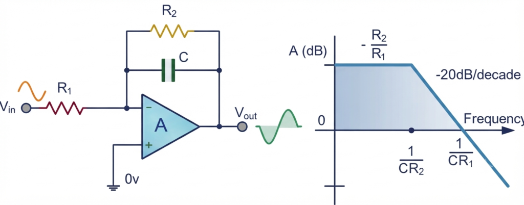
An AC Op-Amp Integrator Amplifier processes alternating input signals and produces an output based on their time integral. Unlike the basic DC integrator, which can convert a square-wave input into a triangular waveform, the AC integrator produces a sinusoidal output from a sinusoidal input with a phase shift of approximately .
When a triangular waveform is applied at the input, the circuit can produce a sinusoidal waveform at the output. This waveform-shaping behavior also forms the basis of an active low-pass filter, whose cutoff or corner frequency depends on the resistor and capacitor values used in the circuit.
AC Op-amp Integrator Gain
Characteristics of an Op-Amp Integrator
An Op-Amp Integrator Amplifier has several characteristics that determine how effectively it performs signal integration:
- Integration of input signals: The circuit produces an output proportional to the time integral of the input voltage. The output polarity is opposite to that of the input because the circuit uses an inverting configuration.
- Frequency-dependent operation: The feedback capacitor makes the circuit response dependent on input frequency. Its capacitive reactance is given by:. As the input frequency increases, decreases. This causes the circuit gain to decrease with increasing frequency.
- Low-pass behavior: The ideal integrator has a gain magnitude that decreases at approximately 20 dB per decade as frequency increases. Therefore, its frequency response resembles that of a low-pass circuit.
- Phase shift: The integration process introduces a phase relationship between the input and output signals. For a sinusoidal input, the output is shifted by approximately .
- Waveform conversion: The circuit can perform useful waveform transformations. For example, a square-wave input can produce a triangular-wave output, while a sine-wave input produces a cosine-type output.
Limitations of an Op-Amp Integrator
A practical Op-Amp Integrator Amplifier cannot achieve the ideal performance because of limitations in the op-amp, capacitor, and other circuit components:
- Finite op-amp gain and bandwidth: A practical op-amp has limited open-loop gain and bandwidth. These limitations restrict the frequency range over which accurate integration can occur.
- Input bias current: Small bias currents flowing into the op-amp input terminals produce additional voltage drops across . These currents introduce errors in the output voltage.
- Offset voltage: The op-amp’s input offset voltage can cause an unwanted output voltage and may gradually drive the integrator toward saturation.
- Capacitor leakage: A practical capacitor has finite leakage resistance. Leakage current can discharge the capacitor and cause the output voltage to drift from its expected value.
- Output saturation: At very low frequencies or with a large input signal, the integrator gain can become sufficiently high to drive the output beyond the op-amp’s available output range. This can result in saturation or clipping.
- Component tolerances: Variations in the values of and affect the integration constant and therefore introduce errors in the output.
- Noise and distortion: Op-amp noise, capacitor imperfections, and other non-ideal characteristics can affect the accuracy of the integrated output signal.
How to Design an Op-Amp Integrator?
Designing an Op-Amp Integrator Amplifier requires selecting suitable values for the input resistor , feedback capacitor , and op-amp according to the input signal and required output. The following factors should be considered during the design:
1. Integration Time Constant
The integration time constant is determined by the product of the input resistance and feedback capacitance:
It determines how quickly the capacitor responds to changes in the input signal. A larger value results in slower integration, while a smaller value produces faster integration.
The time constant should be selected according to the frequency, duration, and amplitude of the input signal. It should also provide sufficient accuracy while preventing excessive output drift or saturation.
2. Output Voltage Range
The output voltage depends on the input signal, integration time constant, and op-amp supply voltage. The output must remain within the allowable output swing of the selected op-amp. If the output reaches the supply limits, the op-amp can saturate and distort the integrated waveform.
Therefore, select and so that the expected output remains within the safe operating range, with sufficient margin for signal variations and circuit errors.
3. Op-Amp Characteristics
The selected op-amp should have suitable open-loop gain, bandwidth, input impedance, output drive capability, input offset voltage, input bias current, and noise performance for the intended application. These parameters affect the accuracy and stability of the integration process.
The op-amp’s datasheet specifications should be checked over the expected operating frequency, supply voltage, and temperature range before finalizing the design.
Examples of Op-Amp Integrators
The following examples illustrate how different combinations of and can produce the same integration time constant while accommodating different input and output voltage ranges. The examples use a Texas Instruments TLV9002 op-amp with a supply voltage of .
Example 1: R=20kΩ, C=0.05μF
For this Op-Amp Integrator Amplifier, the integration time constant is:
This time constant allows the circuit to integrate input signals with frequencies up to approximately 100 Hz effectively.
Assuming an input voltage range of , the estimated output voltage range is:
The frequency response decreases at approximately 20 dB per decade, beginning around 100 Hz and extending toward the upper operating limit determined by the op-amp’s gain-bandwidth product (GBW).
Example 2 : R=50kΩ, C=0.02μF
In this configuration:
Although the resistor and capacitor values differ from Example 1, their product remains the same. Therefore, the integration time constant is also 1 ms, giving a similar basic integration response.
For an assumed input range of , the estimated output range is:
The integrator response begins around 100 Hz, with the practical upper frequency limit depending on the selected op-amp and its GBW.
Example 3 : R=5kΩ, C=0.02μF
The integration time constant for this circuit is:
Again, the product of and remains 1 ms, so the circuit provides the same nominal integration time constant as the previous examples.
If the input voltage varies within , the estimated output voltage range is:
The frequency response follows the integrator characteristic with an approximate 20 dB-per-decade roll-off. The actual upper frequency limit depends on the op-amp’s gain, bandwidth, and other practical circuit limitations.
Comparison of the Examples
| Example | R | C | RC | Assumed Input Range | Estimated Output Range |
| 1 | 20 kΩ | 0.05 μF | 1 ms | ±2 V | ±0.2 V |
| 2 | 50 kΩ | 0.02 μF | 1 ms | ±1 V | ±0.1 V |
| 3 | 5 kΩ | 0.2 μF | 1 ms | ±3 V | ±0.3 V |
These examples show that different resistor and capacitor combinations can produce the same integration time constant when their product remains constant. However, the selected component values and input signal range influence the practical operating conditions and output voltage of the Op-Amp Integrator Amplifier.
How to Improve an Op-Amp Integrator?
A practical Op-Amp Integrator Amplifier can experience output drift, saturation, and limited frequency response because of the non-ideal characteristics of the op-amp and feedback capacitor. Adding suitable components to the feedback network can improve stability and extend the useful operating range.
Adding a Parallel Resistor with the Feedback Capacitor
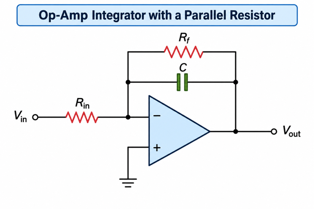
A resistor connected in parallel with the feedback capacitor limits the low-frequency gain of the integrator. This modification prevents the output from increasing excessively at very low frequencies and reduces the possibility of op-amp saturation caused by DC offsets, bias currents, and capacitor leakage.
The effective feedback impedance is the parallel combination of and the capacitive reactance . Therefore, the voltage gain can be expressed as:
where is the combined impedance of and .
At DC, the capacitor behaves approximately as an open circuit, so the feedback is provided mainly by . The maximum low-frequency gain is therefore approximately:
As the frequency increases, the capacitive reactance decreases and the circuit increasingly exhibits integrator behavior. The transition occurs around the corner frequency:
Choosing an appropriate value of helps prevent saturation while maintaining the required integration range.
Adding a Resistor in Series with the Capacitor
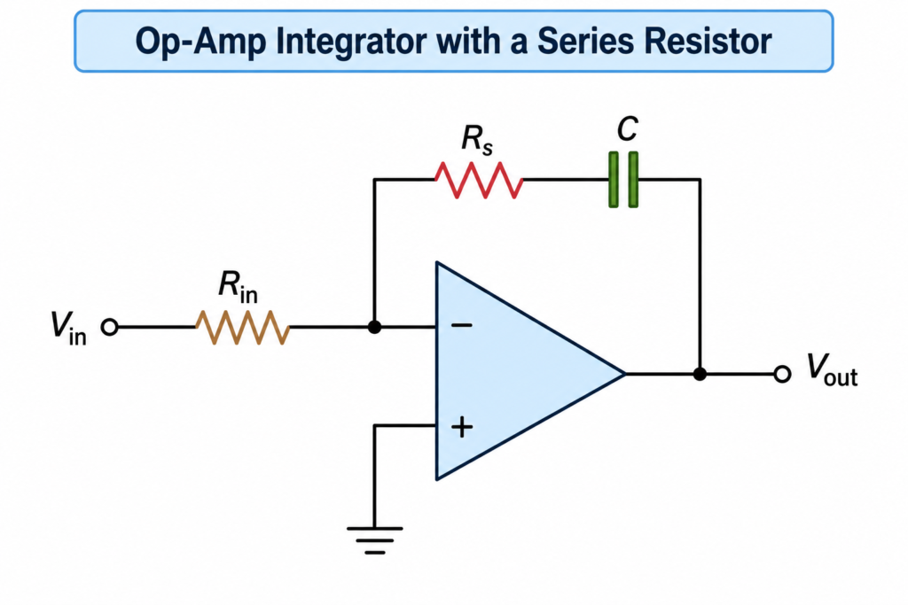
Another method of modifying an Op-Amp Integrator Amplifier is to place a resistor in series with the feedback capacitor. This resistor limits the feedback current and can reduce the influence of input bias current on the output.
The resulting feedback impedance is:
The series resistor also changes the frequency response of the circuit by introducing an additional frequency-dependent characteristic. The values of , , and determine the resulting gain and useful operating range.
Selecting Suitable R and C Values
The values of and directly determine the integration constant:
A suitable combination should provide the required integration response without driving the op-amp into saturation. The component values should also be selected according to the input frequency, signal amplitude, op-amp bandwidth, and required accuracy.
These modifications make the practical Op-Amp Integrator Amplifier more stable and usable over a defined frequency range while reducing the effects of DC errors and other non-ideal characteristics.
Applications of Op-Amp Integrator Amplifier
The Op-Amp Integrator Amplifier is widely used in analog electronics because it can integrate an input signal and generate a corresponding output waveform. Common applications include:
- Waveform Generation – Converts square-wave signals into triangular waveforms and performs other waveform-shaping operations.
- Active Low-Pass Filters – Provides frequency-selective filtering and attenuates higher-frequency signals.
- Analog Computers – Performs mathematical integration for solving differential equations and other analog computation tasks.
- Signal Processing – Integrates and processes time-varying signals in analog signal-processing circuits.
- Analog-to-Digital Converters (ADCs) – Integrators are used in several ADC architectures to accumulate and process input signals.
- Ramp and Sweep Generators – Produces ramp or sweep voltages from constant or pulsed input signals.
- Control Systems – Used in integral control circuits to reduce steady-state error and improve control-system response.
- Wave-Shaping Circuits – Converts one waveform into another by exploiting the mathematical relationship between a signal and its integral.
- Function Generators – Forms part of waveform-generation circuits that produce triangular, ramp, and related signals.
- Integrator-Based Measurement Circuits – Accumulates signals over time for measurement and monitoring applications.
Conclusion
An Op-Amp Integrator Amplifier is an important analog circuit that performs mathematical integration using an input resistor and a feedback capacitor. Its output depends on the accumulated input signal and provides useful waveform-shaping capabilities. Practical modifications, such as adding a resistor in parallel with the feedback capacitor or a resistor in series with it, can improve stability, control the frequency response, and reduce the effects of non-ideal characteristics.
By selecting suitable resistor, capacitor, and op-amp values, the integrator can provide reliable performance across the required operating frequency and voltage range. These characteristics make the Op-Amp Integrator Amplifier useful in signal processing, waveform generation, filtering, analog computation, and other analog electronic applications.
Read Next:
- Inverting vs Non-Inverting Amplifier: Differences, Gain, and Applications
- Inverting Operational Amplifier: Circuit, Working, and Gain Formula
- Op-Amp Building Blocks: Basic Circuits and Applications
- Operational Amplifier (Op-Amp): Basics, Types, Working & Applications
- Non-inverting Operational Amplifier: Circuit, Gain & Formula
- Summing Amplifier: Circuit, Gain Formula, Derivation & Applications
- Differential Amplifier: Circuit, Types, Formula & Applications
- Op-Amp Differentiator Amplifier: Circuit, Working, Formula & Applications
- Op-Amp Multivibrator: Working, Circuit, Types & Applications
- Op-Amp Comparator: Circuit, Working, Formula, Hysteresis & Applications
- Op-Amp Monostable Multivibrator: Circuit, Working, Formula & Timing