An Op-Amp Monostable Multivibrator is a one-shot circuit that remains in a stable state until an external trigger is applied. The trigger causes the circuit to generate a single output pulse with a predetermined duration, after which it automatically returns to its original stable state.
Op-amp Monostable Circuit
Simple monostable multivibrator circuits can be built using discrete electronic components or digital logic gates. An operational amplifier can also be configured to perform the same function, forming an Op-Amp Monostable Multivibrator, commonly called a one-shot circuit.
An op-amp monostable is a regenerative switching circuit that has one stable operating state. When an external trigger is applied, the circuit temporarily leaves this stable state and generates a single output pulse. The output remains in this temporary state for a predetermined interval before automatically returning to its original condition.
The duration of the output pulse is mainly controlled by the RC timing network. By selecting suitable values of the resistor and capacitor, the pulse width can be set to the required value, ranging from microseconds to milliseconds or even seconds.
After the timing interval has elapsed, the circuit returns to its stable state and remains there until another trigger signal is received. Thus, each trigger produces one well-defined output pulse.
The basic operating sequence of an op-amp monostable can be represented by the following block diagram:
Trigger Signal → Op-Amp Monostable → Timed Output Pulse
The circuit is useful whenever a short, controlled-duration pulse is required in response to an external event.
Op-amp Monostable Block Diagram
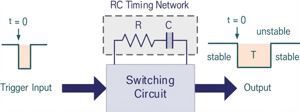
The basic block diagram of a monostable multivibrator consists of a switching circuit together with an external resistor and capacitor that form the timing network. The switching element may be implemented using transistors, digital logic gates, or an operational amplifier.
The resistor and capacitor determine the circuit’s time constant:
This time constant controls how quickly the capacitor charges or discharges and, consequently, determines the duration of the output pulse .
In this tutorial, we will develop a basic Op-Amp Monostable Multivibrator using an op-amp comparator with a positive feedback network. The positive feedback makes the circuit regenerative, meaning that a change at the input is reinforced by a portion of the output being fed back to the input.
When a suitable trigger is applied, the positive feedback causes the op-amp output to switch rapidly to the opposite state. The capacitor then charges or discharges through the timing resistor. Once the capacitor voltage reaches the required threshold, the comparator changes state again and the circuit returns automatically to its stable condition.
Thus, the combination of positive feedback and an RC timing network allows the op-amp monostable to generate a single output pulse of controlled duration in response to each trigger signal.
An Op-Amp Monostable Circuit
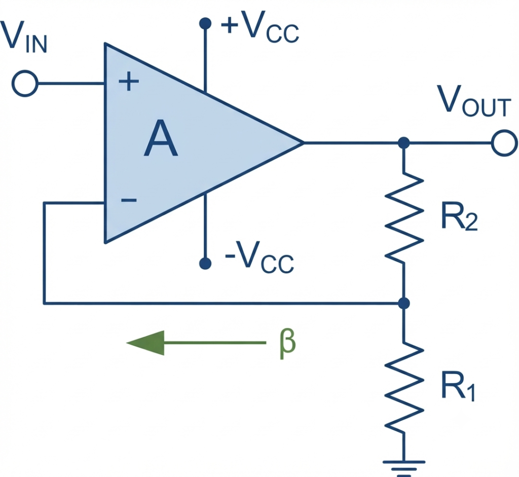
To understand the operation of an op-amp monostable multivibrator, it is useful to first consider a conventional inverting amplifier configuration.
In an inverting amplifier, a portion of the output voltage is returned to the inverting input through the feedback resistor network. This is known as negative feedback because the feedback signal opposes changes in the input. Negative feedback keeps the differential input voltage very small and allows the op-amp to operate in its linear region.
The output of the inverting amplifier is also 180° out of phase with the input. An increase in the voltage applied to the inverting input causes the output voltage to move in the opposite direction. This negative-feedback action provides stable and controlled amplification.
Now consider reversing the input connections so that the feedback signal is applied to the non-inverting (+) input. The feedback is then positive rather than negative. Instead of opposing a change in the output, positive feedback reinforces it. This regenerative action causes the op-amp to operate as a comparator with hysteresis, commonly known as a Schmitt trigger.
The op-amp monostable circuit is based on this Schmitt-trigger configuration. Resistors and provide the positive feedback required to establish the upper and lower switching thresholds. These thresholds give the circuit its hysteresis and allow it to remain in a defined state until a suitable trigger is applied.
Positive feedback also gives the circuit state-dependent switching behavior. The output state influences the threshold at which the next transition occurs. When an RC timing network is added to this Schmitt-trigger arrangement, th
The basic op-amp voltage comparator with positive feedback is shown below and forms the foundation of the monostable circuit.
Op-Amp Schmitt Comparator
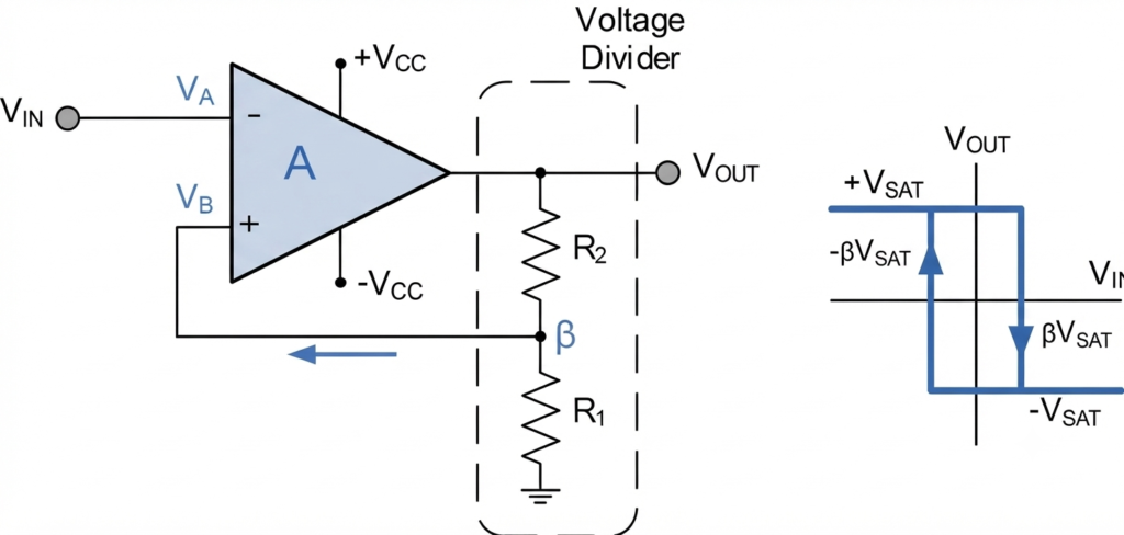
In the op-amp Schmitt comparator, a pair of resistors forms a positive-feedback network between the op-amp output and its non-inverting input. This network determines the switching thresholds and provides the hysteresis required for stable operation.
When the op-amp output is driven toward the positive supply rail, , a positive feedback voltage appears at the non-inverting input. The voltage at this input therefore becomes positive with respect to ground.
When the output switches toward the negative supply rail, , the polarity of the feedback voltage reverses. The non-inverting input then receives a negative voltage relative to ground.
The two resistors form a voltage-divider network, so only a fraction of the output voltage is fed back to the non-inverting input. Let this feedback voltage be . Its magnitude depends on the ratio of the two resistors.
The feedback fraction, represented by , can be expressed as:
Therefore, the voltage appearing at the non-inverting input is:
When the output changes polarity, also changes polarity. These two possible feedback voltages establish the Upper Trip Point (UTP) and Lower Trip Point (LTP) of the Schmitt comparator.
This positive-feedback arrangement is important in the op-amp monostable circuit because it provides well-defined switching thresholds. When combined with an RC timing network, these thresholds determine when the capacitor voltage causes the comparator to change state and generate the required output pulse.
Feedback Fraction, β Formula
The feedback fraction determines how much of the op-amp output voltage is returned to the non-inverting input. For the resistor arrangement shown, it is given by:
The value of does not have to remain fixed. Resistors and can be replaced by a potentiometer, with its wiper connected to the non-inverting input of the op-amp. Adjusting the wiper position changes the voltage-divider ratio and therefore allows the feedback fraction to be varied.
The value of directly influences the hysteresis of the Schmitt trigger. Increasing the feedback fraction increases the separation between the switching thresholds, while decreasing reduces the hysteresis band.
A very small value of should generally be avoided because it produces only a narrow hysteresis range. In this condition, electrical noise or small input variations near the switching threshold may cause unwanted or repeated output transitions.
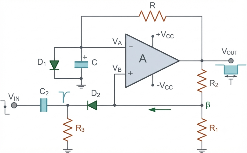
To convert the Schmitt trigger into an op-amp monostable multivibrator, an additional feedback path containing a resistor and capacitor is connected between the output and the inverting input.
This RC timing network feeds a time-varying voltage back to the inverting input. After the circuit is triggered, the capacitor begins to charge or discharge through the resistor. When the capacitor voltage reaches the switching threshold established by the positive-feedback network, the op-amp changes state.
Thus, the positive-feedback network determines the switching threshold, while the RC network controls the time interval before switching occurs. Together, these two networks allow the circuit to generate a single output pulse of a predetermined duration.
Basic Op-Amp Monostable Circuit Diagram
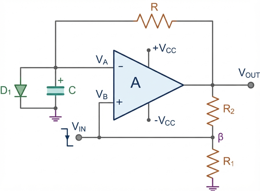
When power is first applied to the circuit at , the op-amp output quickly moves toward one of its saturation levels. Because of the positive feedback provided by the Schmitt-trigger network, the output can initially settle at either or . For this analysis, assume that the output settles at the positive supply rail:
The positive feedback network then establishes the voltage at the non-inverting input as:
where is the feedback fraction.
At the inverting input, diode maintains the voltage near its forward voltage of approximately . Thus:
Since , the op-amp remains in its stable state with the output at . The capacitor also charges to approximately and remains at this level while is forward biased.
Applying the Trigger
When a suitable negative trigger pulse is applied to the circuit, the voltage at the non-inverting input is driven below the existing feedback voltage. The relationship between the two input voltages therefore reverses, causing the Schmitt-trigger stage to switch.
The op-amp output moves rapidly from to . Consequently, the feedback voltage also changes polarity:
The circuit has now entered its temporary or quasi-stable state.
RC Timing Action
After the output switches negative, the capacitor begins to change its voltage through the timing resistor . The capacitor voltage moves exponentially from its initial value of approximately toward the negative output level.
The diode is now reverse biased and therefore no longer affects the timing process. The capacitor voltage changes according to the RC time constant:
As the capacitor voltage moves downward, it eventually reaches the negative switching threshold:
At this point, the Schmitt trigger changes state again. The op-amp output returns to its original stable condition at .
The complete sequence therefore consists of three main stages: stable state → triggered quasi-stable state → automatic return to the stable state. The duration of the temporary state is determined primarily by the timing network.
When the output returns to , the capacitor attempts to charge in the opposite direction. However, diode becomes forward biased and clamps the capacitor voltage to approximately . The capacitor is therefore reset and the circuit is ready for the next trigger pulse.
The capacitor voltage and output waveform during this process can be represented graphically as shown below.
Op-Amp Monostable Waveforms Diagram
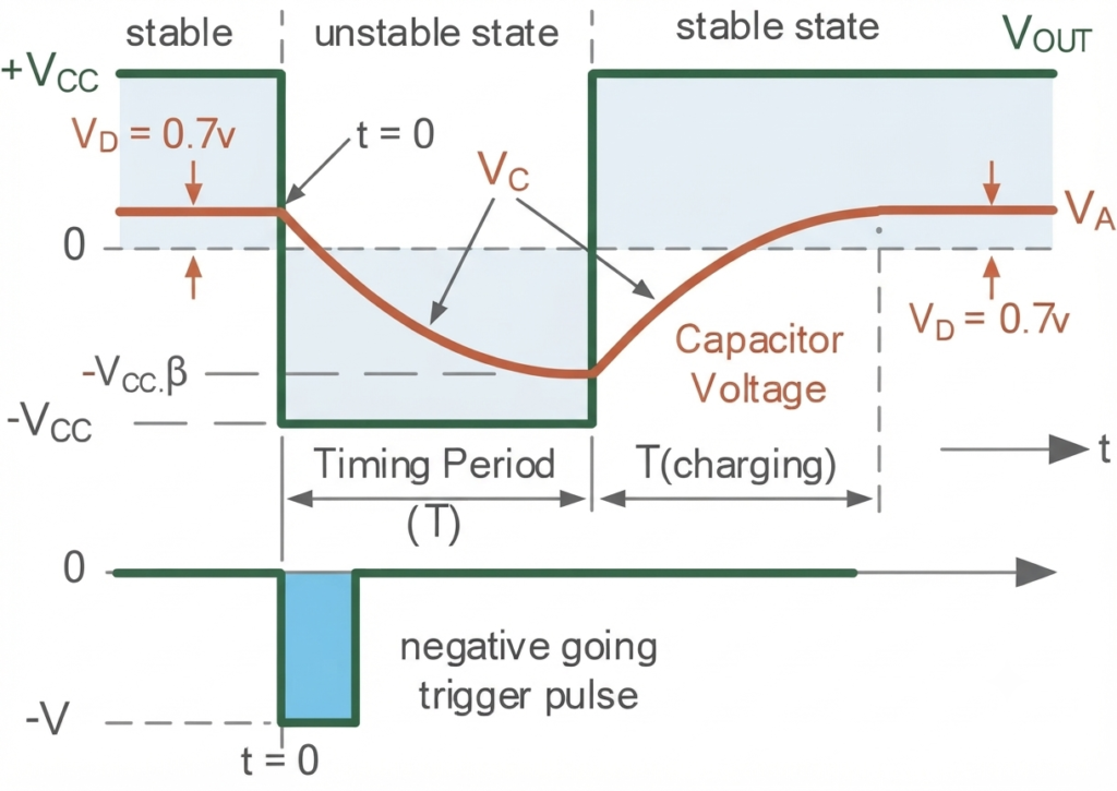
The waveform above shows the operation of an op-amp monostable circuit following the application of a negative-going trigger pulse. The trigger causes the circuit to leave its normal stable state and enter a temporary unstable state.
During this interval, the capacitor charges through the feedback resistor . After a time interval , the capacitor voltage reaches the required switching level, causing the op-amp to return automatically to its original stable state.
The time interval represents the duration of the rectangular output pulse, or the time for which the circuit remains in its temporary unstable state.
This pulse duration is determined by the RC timing network and is given by:
Monostable Timing Period
If the two feedback resistors of the operational amplifier have equal values, that is, , the above equation can be simplified to:
The capacitor requires a certain amount of time to recharge from to (approximately 0.7 V). During this recovery period, a second negative trigger pulse cannot initiate a new timing cycle.
Therefore, for the op-amp monostable circuit to operate correctly when the next trigger pulse is applied, the time interval between two successive trigger pulses, , must be greater than the sum of the timing period and the capacitor charging recovery time .
Charging Recovery Time
The charging recovery time is therefore given by:
Where is the supply voltage, is the forward voltage drop of the diode, usually around 0.6 to 0.7 V, and is the feedback fraction.
To ensure that the op-amp monostable circuit receives a suitable negative trigger pulse at the leading edge of the negative-going input signal, while also preventing false triggering when the circuit is in its stable state, an RC differentiating circuit can be added to the input.
A differentiator circuit produces a sharp negative output spike from a square or rectangular input waveform. This sudden reduction in the comparator’s threshold voltage below its feedback fraction, , triggers the op-amp monostable and starts its timing period. The differentiator circuit is formed using a resistor-capacitor (RC) network, as shown.
RC Differentiator Circuit
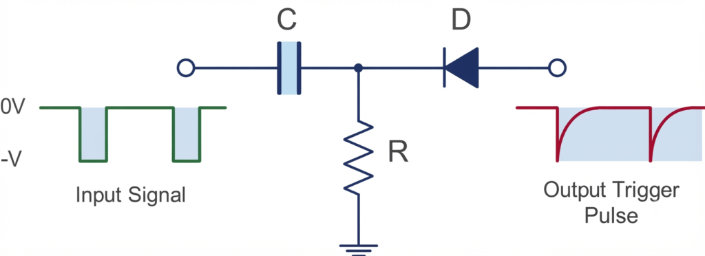
The basic differentiator circuit shown above uses another resistor-capacitor (RC) network, in which the output voltage is proportional to the rate of change of the input voltage with respect to time. When the input voltage changes from 0 to , the non-polarised capacitor begins to charge exponentially.
Since the capacitor voltage, , is initially zero, the output of the differentiator immediately changes from 0 to , producing a negative spike. As the capacitor continues to charge, this spike gradually decays exponentially.
In a typical RC differentiator circuit, the peak value of the negative spike is approximately equal to the magnitude of the trigger waveform. As a general rule, to obtain sharp and narrow spikes, the time constant should be at least ten times smaller than the input pulse width. For example, if the input pulse width is 10 ms, the time constant should be less than 1 ms, or 10% of the pulse width.
The main advantage of using a differentiator circuit is that it blocks constant DC voltages and slowly varying signals, allowing only rapidly changing trigger pulses to initiate the monostable timing period. Diode ensures that the trigger pulse applied to the op-amp’s non-inverting input is always negative.
Adding the RC differentiator circuit to the basic op-amp monostable circuit gives:
Op-amp Monostable Circuit
Worked Example on Op-amp Monostable Multivirator
An op-amp monostable circuit is constructed using the following components: , , and .
If the op-amp monostable is supplied from a supply and the timing period is initiated by a 8 ms negative trigger pulse, calculate the circuit’s timing period, capacitor recovery time, minimum time between trigger pulses, and differentiator network values.
Also, draw the completed circuit.
Data Given:
- Supply voltage =
- Trigger pulse width =
1. Timing Period, (T)
2. Capacitor recovery time:
Using the recovery-time equation:
Substituting the values:
3. Total Time Between Trigger Pulses
The minimum time between successive trigger pulses must be greater than the sum of the timing period and the capacitor recovery time.
Using the values calculated above:
Therefore, the time between successive trigger pulses should be greater than approximately 73 ms to ensure proper operation of the op-amp monostable circuit.
4. Differentiator Network Values
The input pulse width is 8 ms. Therefore, the desired negative spike duration is approximately 10% of the input pulse width:
If we assume a capacitance value of , the differentiator RC values can be calculated using the time constant:
Therefore,
Thus, the differentiator network can use:
This gives the final Op-Amp Monostable circuit for our example as:
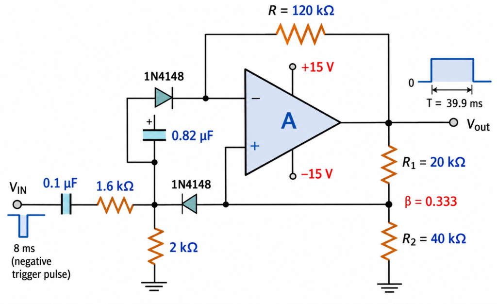
Conclusion
In this tutorial, we have seen how an Op-Amp Monostable circuit can be constructed using a general-purpose operational amplifier, such as the 741, along with a few external components.
Although monostable (one-shot) multivibrator circuits can be constructed more easily using discrete components, digital logic gates, or a commonly used 555 Timer IC, an op-amp-based monostable circuit can be useful in analogue applications where an operational amplifier is already being used.
By configuring the op-amp as a Schmitt trigger with positive feedback, the duration of the output pulse is determined by the time constant of the RC timing circuit and the resistor ratio of the voltage-divider network. This voltage-divider network provides the positive feedback required for the circuit to switch between its stable and temporary states, thereby producing the required output pulse.
Read Next:
- Inverting vs Non-Inverting Amplifier: Differences, Gain, and Applications
- Inverting Operational Amplifier: Circuit, Working, and Gain Formula
- Op-Amp Building Blocks: Basic Circuits and Applications
- Operational Amplifier (Op-Amp): Basics, Types, Working & Applications
- Non-inverting Operational Amplifier: Circuit, Gain & Formula
- Summing Amplifier: Circuit, Gain Formula, Derivation & Applications
- Differential Amplifier: Circuit, Types, Formula & Applications
- Op-Amp Integrator Amplifier: Formula, Working & Applications
- Op-Amp Differentiator Amplifier: Circuit, Working, Formula & Applications
- Op-Amp Multivibrator: Working, Circuit, Types & Applications
- Op-Amp Comparator: Circuit, Working, Formula, Hysteresis & Applications
- Passive Averager: Circuit, Equation & Op-Amp Averager