This article aims to demonstrate the implementation of a basic NOT gate using the NAND gate. A universal gate is a logic gate that can implement other logic gates. In simpler terms, using a universal gate, one can perform all the fundamental operations such as AND, OR, NOT, NAND, and NOR. The most commonly used universal gates are NAND gates and NOR gates. These gates are considered universal as they can be used to create all other logic gates.
Let us discuss what the NOT and NAND gates are.
What is NOT Gate?
The NOT gate, also known as the inverter, is a fundamental component of digital electronics. This gate has one input and one output, and its function is to take the input signal and produce a logical inversion of it at the output. In simpler terms, it reverses the input signal. This gate is particularly important in digital logic when we require the output to be the opposite of the input.
The behavior of a NOT gate can be summarized as follows:
- If the input is equal to 1, then the output will be 0
- If the input is equal to 0, then the output will be 1
Symbol of NOT Gate
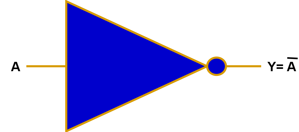
The NOT gate, also known as an inverter, is represented by a triangle with a small circle at the input end to indicate the inverting function.
The symbol indicates:
- The Triangle shows a gate.
- The circle at the triangle indicates the inversion operation, which means the input is inverted.
- ‘A’ represents the input signal, whereas the complement of ‘A’ represents the output.
Truth Table of NOT Gate
The truth table for a NOT gate can be represented as follows
| Input(A) | Output(Y=Ā) |
| 0 | 1 |
| 1 | 0 |
NOT gate is used in electronic circuits to design logic gates in devices such as transistors and diodes.
What is NAND Gate?
A NAND gate is a simple digital logic gate that represents the operation of “NOT-AND.” It generates an output that is the opposite of the AND operation. If both inputs are high (1), the output is low; otherwise, it is high for all other inputs. The NAND gate comprises an AND gate and a NOT gate that complement each other. This is significant because any Boolean function can be implemented using a combination of NAND gates.
Symbol of NAND Gate
The behavior of a NAND gate can be summarized as follows:
- When all the inputs are true (1), the output becomes false (0).”
- If one or all inputs are false (0), the output is true (1).
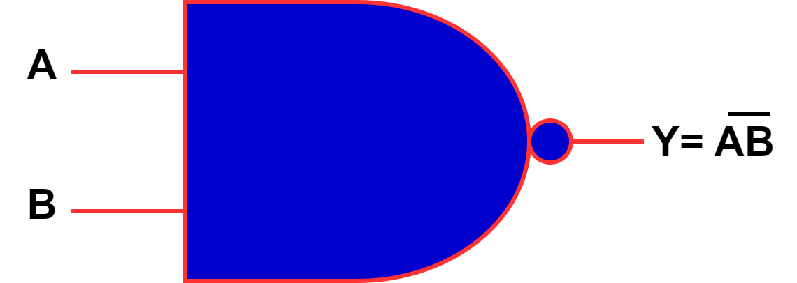
The symbol indicates that it is an AND gate with an inversion, which means that it performs the AND operation on the input and then negates or complements the result to produce the NAND operation output.
Truth Table of NAND Gate
The truth table for a NAND gate is presented below:
| Input A | Input B | Output Y |
| 0 | 0 | 1 |
| 0 | 1 | 1 |
| 1 | 0 | 1 |
| 1 | 1 | 0 |
The output of a NAND Gate is false (0) only when both inputs are high; otherwise, it is true for all other inputs. NAND gates can be used in electronic circuits to design logic gates, such as transistors, diodes, or combination circuits.
A NAND Gate produces a false (0) output only when both inputs are high(1). Otherwise, it produces a true(1) output for all other inputs. This gate is widely used in electronic circuits for various devices like transistors and diodes or in combination circuits for designing logic gates.
Implementation Of NOT Gate Using NAND Gate
You know that the NAND gate is really useful. It’s a universal gate, which means you can use it to implement any basic gate. And if you’re looking to create a NOT gate, I can show you how to do it using a NAND gate.
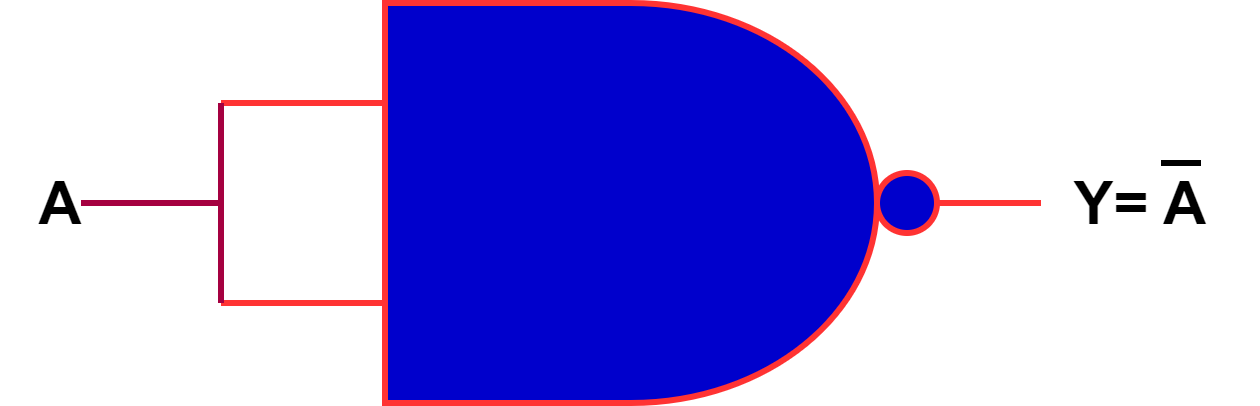
NOT Gate using NAND Gate
By looking at the diagram, we can see that to implement a NOT gate using a NAND gate, we need to connect both inputs of the NAND gate to create a single input for the NOT gate. Then, we take the output of the NOT gate from the output of the NAND gate. After joining both inputs of the NAND gate, the output is (AA)’, which can be simplified to A’ using Boolean algebra.
Truth Table of NOT Gate using NAND Gate
| A | B | Y=(AB)’=A’ |
| 0 | 0 | 1 |
| 1 | 1 | 0 |
The above setup complements the input; thus, a NAND gate is used to implement a NOT gate.
Conclusion
The NOT gate is the fundamental building block of digital logic design and finds its application in various fields, such as arithmetic, storage devices, and control circuits. It collaborates with other gates to perform complex logic operations. Employing NAND gates ensures high performance, capacity, and a deep understanding of digital content. It exhibits the tremendous versatility and power of NAND gates in digital electronic gadgets and offers an electronic design model.
Read Next: