N-Type Semiconductor has a large number of free electrons and it is formed by adding small amount of Pentavalent impurity to a pure semiconductor .
Semiconductors are materials whose electrical properties lie between those of insulators and conductors. They are the backbone of modern electronics, enabling the development of transistors, diodes, solar cells, and various other devices. N-type semiconductors, in particular, play a crucial role in the functionality of these devices. This article will explore what n-type semiconductors are, their energy band diagrams, and how conduction occurs in these materials.
What is an N-type semiconductor?
An n-type semiconductor is created by doping a pure semiconductor crystal, such as silicon or germanium, with an impurity element that has more valence electrons than the semiconductor itself. Typically, these dopants are pentavalent (five-valence electrons), such as phosphorus, arsenic, or antimony. When these elements are introduced into the semiconductor lattice, four of their electrons form covalent bonds with the semiconductor atoms, but the fifth electron is extra and does not find a bonding partner.
This extra electron is loosely bound to its parent atom, making it relatively free to move through the crystal lattice at room temperature. The presence of these free electrons results in an excess of negative charge carriers, hence the term “n-type” (negative-type) semiconductor.
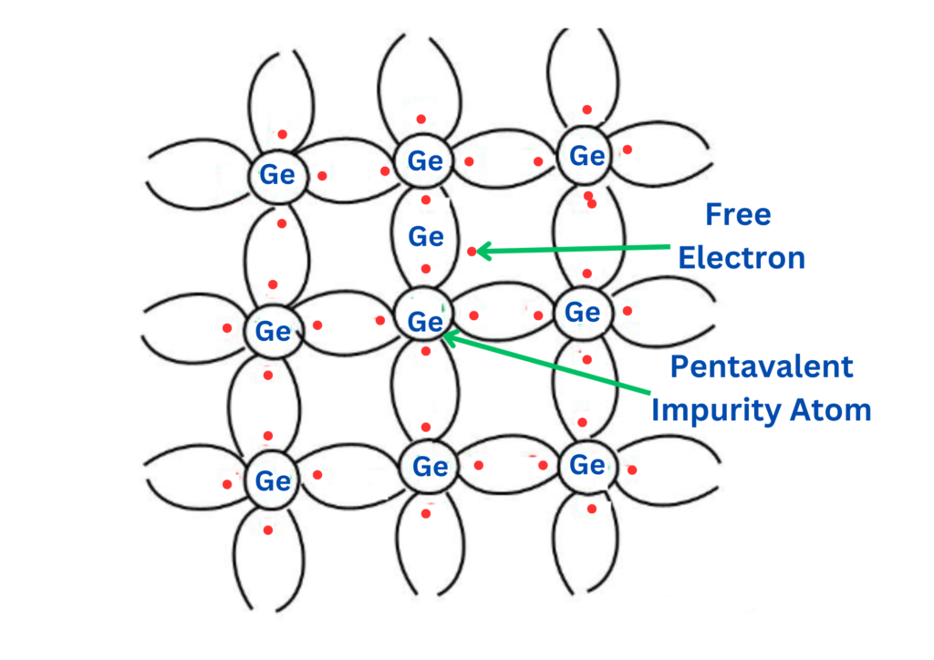
Arsenic, with an atomic number of 33, is classified as 2, 8, 15, and 5. It has five valence electrons, which are added to a germanium crystal. In the figure above, each impurity atom fits into four germanium atoms.
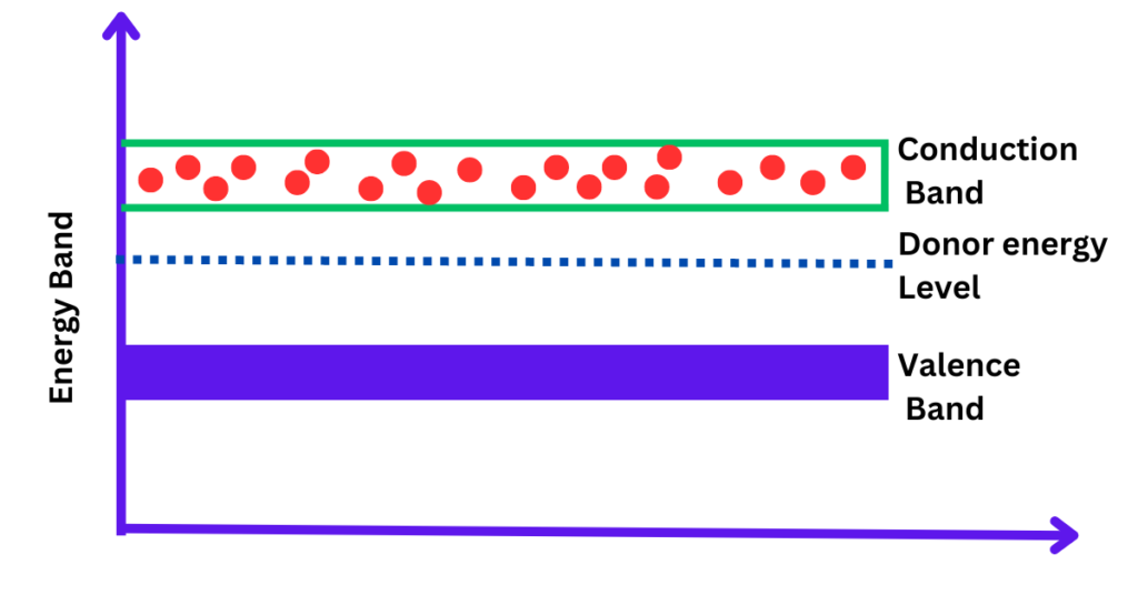
Energy Band Diagram of N-Type Semiconductor
To understand the energy band diagram of an n-type semiconductor, it’s essential to start with the concepts of the conduction band and the valence band:
- Valence Band: This is the highest energy band that can be occupied by electrons at absolute zero temperature. It is fully occupied in a pure semiconductor at this temperature.
- Conduction Band: This is the band above the valence band, and it is typically empty at absolute zero. Electrons in this band are free to conduct electricity.
When a semiconductor is doped with n-type impurities, the extra electrons provided by the dopant atoms create what is known as the donor energy level. This donor level is located just below the conduction band. The energy required to excite an electron from the donor level to the conduction band is much less than the energy needed to excite an electron from the valence band to the conduction band in an intrinsic (undoped) semiconductor.
The energy level diagram for an n-type semiconductor is illustrated in the figure below.
Conduction in N-Type Semiconductors
The conduction process in n-type semiconductors begins with the thermal excitation of electrons. At room temperature, enough thermal energy is available to excite the extra electrons from the donor level into the conduction band. Once in the conduction band, these electrons move freely and contribute to electrical conductivity.
The overall conductivity of an n-type semiconductor is primarily due to the movement of these free electrons, which are the majority carriers. The thermal generation of electron-hole pairs also contributes to conductivity, but to a lesser extent, with holes being the minority carriers in n-type materials.
In an n-type semiconductor, impurity atoms donate free electrons to the conduction band, as shown in the diagram below.
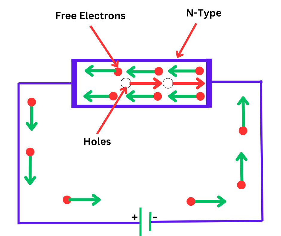
When a potential difference is applied across a certain type of semiconductor, free electrons move toward the positive terminals, creating an electric current. This current flows through the crystal and is carried by the free electrons, which are negatively charged. This type of conductivity is known as negative or n-type conductivity.
The formation of electron-hole pairs and subsequent hole current at room temperature are negligible for most practical applications.
Conclusion
N-type semiconductors are integral to the design and operation of various electronic components. By introducing pentavalent impurities into a semiconductor, engineers can control the conductivity and characteristics of the material, tailoring it to specific applications. The presence of easily excitable electrons near the conduction band allows n-type semiconductors to conduct electricity efficiently, which is vital for the functioning of many electronic devices. Understanding the energy band diagram and conduction mechanism provides insights into how these materials can be manipulated to achieve desired electrical properties in technological applications.