An extrinsic p-type semiconductor is formed by adding a small amount of trivalent impurity to a pure semiconductor. This process creates a large number of holes in the semiconductor material. Trivalent impurities, known as acceptor impurities, such as Gallium and Indium, are added to the semiconductor material to provide a large number of holes.
Acceptor impurities in semiconductors create holes that can accept one electron each, making them p-type semiconductors. This article explores the concept of P-type semiconductors, their energy diagrams, and conduction mechanisms.
Introduction to Semiconductors:
Semiconductors are materials that have electrical conductivity levels that fall between conductors and insulators. Unlike conductors (metals), where electrons can move freely, and insulators, where electrons are tightly bound to atoms, semiconductors exhibit a behavior where their conductivity can be modified by temperature, doping, and external electric fields.
What is P-Type Semiconductor?
P-type semiconductors are semiconductors in which the majority of charge carriers are positively charged “holes” instead of negatively charged electrons. These holes effectively behave as positive charge carriers, contributing to the material’s electrical conductivity. P-type doping involves introducing impurity atoms into the semiconductor crystal lattice, creating excess positive charge carriers.
Formation of P-Type Semiconductor
The process begins with a pure semiconductor crystal. Silicon (Si) and Germanium (Ge) are common semiconductor materials used in electronic devices due to their atomic structure, which allows for controlled manipulation of electrical conductivity.
To create a P-type semiconductor, we introduce certain types of impurity atoms into the crystal lattice. These impurities are called acceptor impurities or trivalent impurities because they create “holes” in the crystal structure, effectively generating positive charge carriers. Boron (B) is a commonly used acceptor impurity in silicon, while Indium (In) and Gallium (Ga) are used in compound semiconductors like Gallium Arsenide (GaAs).
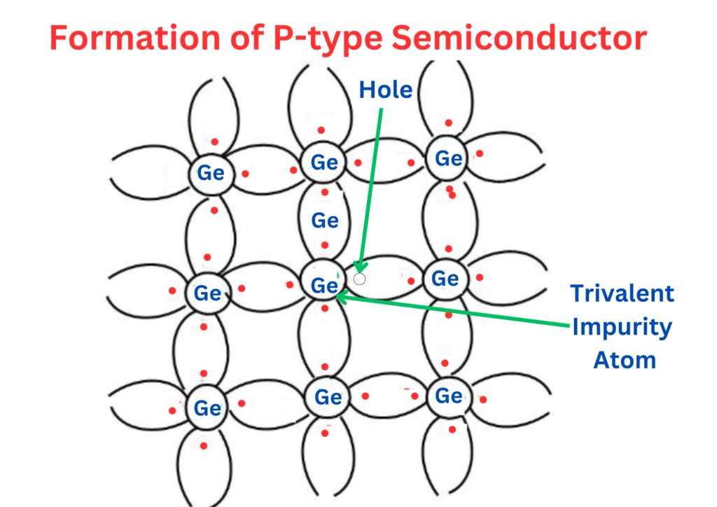
The introduction of acceptor impurities has created an excess of positively charged “holes” in the crystal lattice, making the holes the dominant charge carriers. This results in a material with P-type conductivity, where positive charge carriers (holes) contribute significantly to the electrical conduction.
Energy Band Diagram of a P-Type Semiconductor:
To understand the energy diagram of a P-type semiconductor, let’s consider the band structure. In semiconductors, there are two main energy bands: valence and conduction bands. The valence band is the highest energy band occupied by electrons at absolute zero temperature, while the conduction band is the next higher energy band that electrons can move into when excited.
In a P-type semiconductor, due to the introduction of acceptor impurities (such as boron in silicon), additional energy levels are created close to the valence band. These acceptor impurities have fewer valence electrons than the semiconductor material, leading to “holes” in the valence band. These holes act as mobile charge carriers.
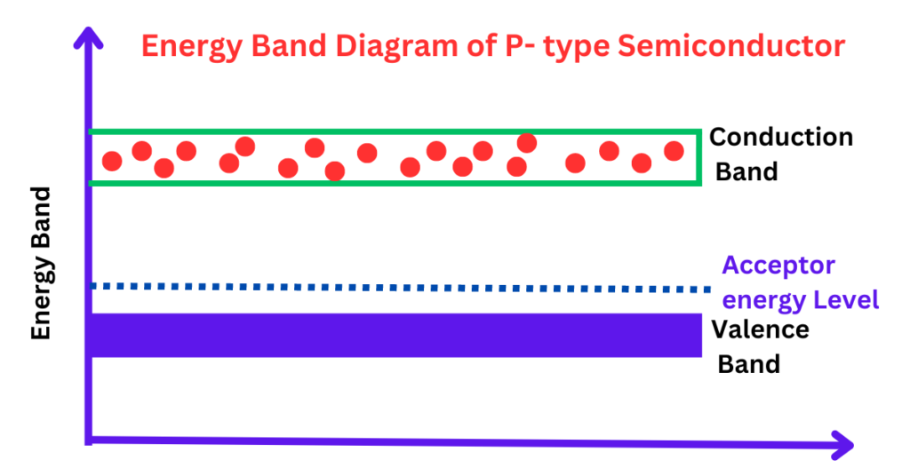
The energy diagram of a P-type semiconductor depicts a downward shift of the Fermi level closer to the valence band due to the presence of acceptor impurities. This shift facilitates the generation of holes, which become the dominant charge carriers in the material.
Conduction Mechanism in P-Type Semiconductors:
The conduction mechanism in P-type semiconductors primarily involves the movement of positively charged holes. When an electric field is applied to the semiconductor material, the holes migrate towards the negative electrode (cathode), creating a flow of positive charge, which constitutes an electric current.
Moreover, P-type semiconductors can undergo minority carrier injection when electrons from the conduction band (minority carriers) are injected into the material. These minority carriers can recombine with the majority carriers (holes) and contribute to the conductivity of the material.
In a p-type semiconductor, the trivalent impurity creates many holes. When a potential difference is applied across this type of semiconductor, holes move towards the positive terminal, as shown in the figure below:
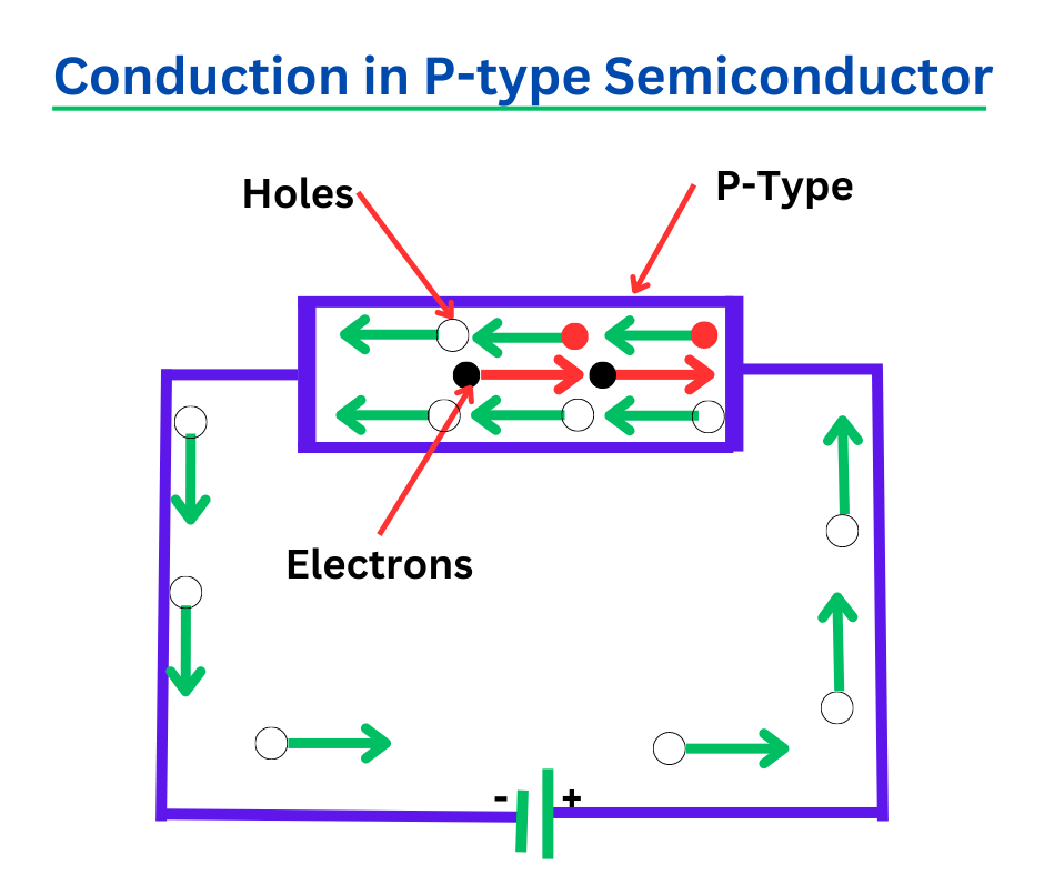
In a crystal, the holes that exist in the valence band move towards the negative terminal, which results in the flow of current through the crystal. As these holes carry positive charge, this type of conductivity is known as positive or p-type conductivity. In p-type conductivity, valence electrons move from one covalent to another.
The conductivity of an n-type semiconductor is almost twice that of a p-type semiconductor. This is because the electrons present in the conduction band of an n-type semiconductor are much more mobile than holes in the valence band of a p-type semiconductor. Holes have poor mobility as they are more tightly bound to the nucleus.
At room temperature, p-type semiconductors generate electron-hole pairs that carry a small amount of current.
P-Type Semiconductor Examples
Examples of p-type semiconductors include boron-doped silicon, aluminum-doped silicon, and boron-doped germanium.
Applications of P-Type Semiconductors:
P-type semiconductors find extensive use in electronic devices such as diodes, transistors, and integrated circuits. They are also essential components in optoelectronic devices like light-emitting diodes (LEDs) and photovoltaic cells.
Conclusion:
P-type semiconductors play a crucial role in the realm of semiconductor physics and technology. By understanding their energy diagram and conduction mechanisms, researchers and engineers can harness their unique properties for a wide range of applications, from electronic circuits to renewable energy devices. As semiconductor technology continues to advance, the importance of P-type semiconductors in shaping our technological landscape remains paramount.