A Non-inverting Operational Amplifier is an op-amp configuration in which the input signal is applied to the non-inverting (+) terminal. The circuit produces an amplified output that remains in phase with the input voltage, meaning the output does not undergo a 180° phase reversal. This configuration uses negative feedback to provide a stable and predictable voltage gain, making it widely used in signal amplification, voltage buffering, and analog electronic circuits.
Introduction to the Non-inverting Operational Amplifier
A non-inverting operational amplifier is an op-amp configuration in which the input voltage, , is connected directly to the non-inverting (+) input terminal. As a result, the output voltage has the same phase as the input signal. When the input voltage increases, the output also increases, producing a positive voltage gain without the 180° phase reversal found in an inverting amplifier.
The circuit uses negative feedback to control and stabilize its voltage gain. A fraction of the output voltage is fed back to the inverting (−) input through a resistor network consisting of and . This feedback arrangement allows the amplifier to maintain a predictable closed-loop gain while improving overall circuit stability.
Under ideal op-amp conditions, the non-inverting configuration has a very high input impedance, theoretically approaching infinity. Therefore, almost no current enters the non-inverting input terminal. It also provides a low output impedance, allowing the circuit to drive connected loads more effectively. These characteristics make the non-inverting operational amplifier useful for voltage amplification, signal conditioning, and buffer applications.
Non-inverting Operational Amplifier Configuration
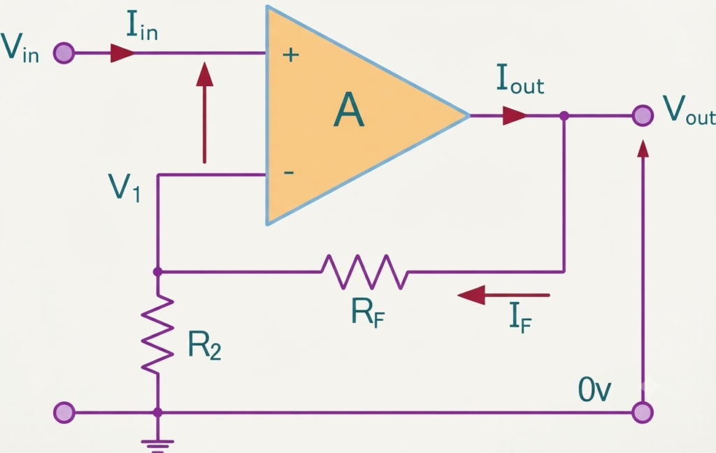
In a non-inverting operational amplifier, the input signal is applied to the non-inverting (+) terminal, while a portion of the output is returned to the inverting (−) terminal through a feedback resistor network. For an ideal op-amp operating with negative feedback, the input currents are assumed to be zero, and the voltages at the two input terminals are approximately equal.
This condition is commonly described as the virtual short concept, where the voltage at the inverting input follows the voltage at the non-inverting input even though the terminals are not physically connected. Since the non-inverting terminal receives , the inverting terminal also approaches the same voltage under normal closed-loop operation.
The feedback resistors and establish the closed-loop voltage gain. Together, they form a feedback network that determines how much of the output voltage is returned to the inverting input. The voltage gain of a standard non-inverting amplifier is therefore controlled primarily by the ratio of these two resistors.
For an ideal non-inverting op-amp, the voltage gain is:
where is the voltage gain, is the feedback resistor, and is the resistor connected between the inverting input and ground.
The resistors and create a simple voltage-divider feedback network, with the amplifier’s voltage gain determined by the ratio between these two resistors as shown below.
Equivalent Potential Divider Network
The feedback resistors in a non-inverting operational amplifier can be represented as an equivalent potential divider. This resistor network determines the fraction of the output voltage that is fed back to the inverting input terminal.
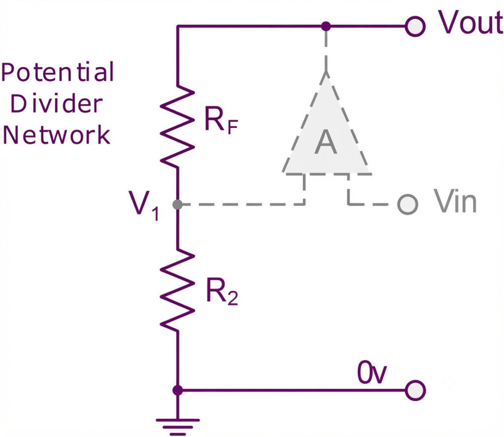
By applying the standard voltage divider equation to this feedback network, we can derive the closed-loop voltage gain of the non-inverting amplifier as follows:
Non-inverting Operational Amplifier Derivation
Using the voltage-divider relationship of the feedback network and the ideal op-amp assumptions, we can derive the closed-loop voltage gain and .
Therefore, the closed-loop voltage gain of a standard non-inverting amplifier is given by:
Ideal Summing Point:
Voltage gain is equal to:
Then,
Transpose to give:
Non-inverting Amplifier Gain Formula
The closed-loop voltage gain of a non-inverting operational amplifier is determined by the ratio of the feedback resistor to the resistor . Unlike an inverting amplifier, the gain is positive because the output signal maintains the same phase as the input signal.
For the standard non-inverting configuration, the voltage gain is:
This equation shows that the voltage gain of a non-inverting amplifier is always equal to or greater than unity, assuming the circuit operates within the op-amp’s linear output range. The minimum gain is 1, which occurs when . Increasing the value of relative to increases the closed-loop voltage gain.
When approaches zero, the ideal closed-loop gain predicted by the equation becomes extremely large. However, a practical operational amplifier cannot provide infinite gain. The actual gain is limited by factors such as the op-amp’s finite open-loop gain, gain-bandwidth product, output voltage limits, and frequency response.
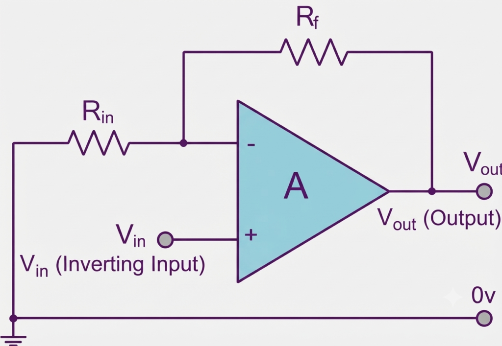
The non-inverting configuration can also be understood by comparing it with the inverting amplifier. The main difference is the point at which the input signal is applied. In the non-inverting arrangement, is connected to the non-inverting (+) terminal, while the resistor network provides negative feedback to the inverting (−) terminal.
Voltage Follower (Unity Gain Buffer)
A voltage follower is a special configuration of a non-inverting operational amplifier in which the feedback resistor is set to zero and the resistor is effectively infinite. The op-amp output is connected directly to its inverting (−) input, creating 100% negative feedback.
With this direct feedback connection, the complete output voltage is returned to the inverting input. The input signal is applied to the non-inverting (+) terminal, so the output follows the input without phase inversion. In other words, the circuit transfers the input voltage to its output while providing a high degree of isolation between the source and the load.
This configuration is commonly known as a unity-gain buffer because it does not provide voltage amplification. Instead, its main purpose is to provide impedance matching and circuit isolation. The voltage follower can therefore connect a high-impedance signal source to a lower-impedance load while minimizing the loading effect on the source.
One of the important characteristics of a voltage follower is its very high input impedance. Under ideal op-amp conditions, the input impedance is considered infinite, so practically no current flows into the input terminal. At the same time, the op-amp provides a very low output impedance, allowing the buffer to drive the next stage with less influence from load changes.
These characteristics make the voltage follower useful in signal buffering, impedance matching, sensor interfaces, analog signal conditioning, and circuit isolation. The voltage relationship and closed-loop gain of this configuration can be derived from the standard non-inverting amplifier equation.
Non-inverting Operational Amplifier Voltage Follower
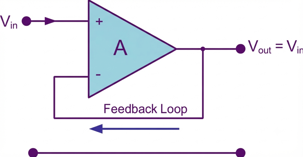
In a non-inverting operational amplifier voltage follower, the output terminal is connected directly to the inverting (−) input terminal. This provides 100% negative feedback, while the input signal is applied to the non-inverting (+) terminal. Under ideal operating conditions, the voltage at the inverting input follows the voltage at the non-inverting input.
Because the output is directly fed back to the inverting input, the voltage follower provides a fixed unity-gain response. The output therefore follows the input signal without phase inversion. The relationship between the input and output voltages can be expressed as:
Therefor Gain
The ideal voltage follower has an extremely high input impedance, theoretically approaching infinity. Consequently, it draws negligible current from the signal source. Its output impedance is very low, allowing the circuit to supply current to the connected load without significantly loading the preceding stage.
These properties make the unity-gain buffer particularly useful when circuit isolation or impedance matching is required rather than voltage amplification. For example, it can be placed between a high-impedance sensor and a lower-impedance circuit to prevent the load from affecting the sensor signal.
In an ideal op-amp model, the input current is zero and the feedback connection carries no current. Therefore, the voltage drop and power dissipation associated with the feedback path are negligible. Practical op-amps, however, have small input bias and leakage currents, along with parasitic capacitances. The feedback arrangement and any additional components must therefore be selected according to the characteristics of the particular op-amp and application.
Voltage followers are widely used for signal buffering, impedance transformation, circuit isolation, sensor interfaces, and active filter circuits. They are also commonly found in multistage analog circuits, including Sallen-Key filter configurations, where buffering helps prevent one circuit stage from significantly affecting another.
The closed-loop gain of the voltage follower can be obtained directly from the standard non-inverting amplifier gain relationship. This provides the basis for understanding why the voltage follower has a unity voltage gain.
Conclusion
The non-inverting operational amplifier is a widely used op-amp configuration in which the input signal is applied to the non-inverting (+) terminal. Unlike an inverting amplifier, the output maintains the same phase as the input signal, so there is no 180° phase reversal.
The closed-loop voltage gain is controlled by the feedback resistor network connected to the inverting (−) terminal. The values of and determine the amount of negative feedback and, consequently, the overall voltage gain of the amplifier. With appropriate component values, the circuit provides stable and predictable amplification.
A non-inverting op-amp also offers very high input impedance and low output impedance, making it useful for applications where the signal source needs to be isolated from the load. Common applications include voltage buffering, signal conditioning, impedance matching, active filtering, and low-level signal amplification.
A special case of this configuration is the voltage follower, in which the output is directly connected to the inverting input. The voltage follower provides unity voltage gain while offering the impedance characteristics of an op-amp buffer.
After understanding single-input op-amp configurations such as the inverting and non-inverting amplifiers, the next step is to examine circuits that accept multiple input signals. A summing amplifier uses an op-amp to combine two or more input voltages and produce a corresponding output signal.
Understanding the non-inverting amplifier therefore provides an important foundation for studying more advanced operational amplifier circuits and analog signal-processing applications.
Read Next:
- Resistors in Parallel – Parallel Connected Resistors Explained
- Resistors in Series: Definition, Formula, Rules, Calculation, and Examples
- Capacitors in Series and Series Capacitor Circuits – Complete Guide
- Voltage Divider: Rule, Equations, Formulas, and Practical Applications
- AC Capacitance: Formula, Reactance & Phase Angle
- Operational Amplifier (Op-Amp): Basics, Types, Working & Applications