A tunnel diode, also known as an Esaki diode, is a type of semiconductor diode that exhibits “negative resistance” due to the quantum mechanical phenomenon called tunneling. Tunnel diodes have a pn junction that is heavily doped and approximately 10 nm wide. This extreme doping results in a broken bandgap, where conduction band electron states on the N-side align with valence band hole states on the P-side.
Due to transit time and other effects, transistors are limited in their application in high-frequency ranges. However, many devices utilize semiconductors’ negative conductance properties for such applications. One such device is the tunnel diode, also known as the Esaki diode, named after L. Esaki for his work on this effect.
The dopant concentration in the p and n regions is extremely high, ranging from 1024 to 1025 m-3. The pn junction is abrupt, resulting in a narrow depletion layer width. When a forward bias is applied, the current-voltage characteristics of a tunnel diode exhibit a negative slope region.
The term “tunnel diode” refers to a phenomenon within the diode due to quantum mechanical tunneling. The diode is heavily doped, so at a temperature of absolute zero, the Fermi levels lie within the bias of the semiconductors.
Characteristics of Tunnel Diode
When a reverse bias is applied to a p-n junction, the Fermi level on the p-side becomes higher than that of the n-side. This leads to the tunneling of electrons from the balance band of the p-side to the conduction band of the n-side. As the reverse bias strength increases, the tunnel current also increases.
When a forward bias is applied, the Fermi level of the n-side becomes higher than the Fermi level of the p-side. This causes the tunneling of electrons from the n-side to the p-side. The amount of current generated by this tunneling is much larger than the normal junction current. As the forward bias increases, the tunnel current also increases to a certain limit.
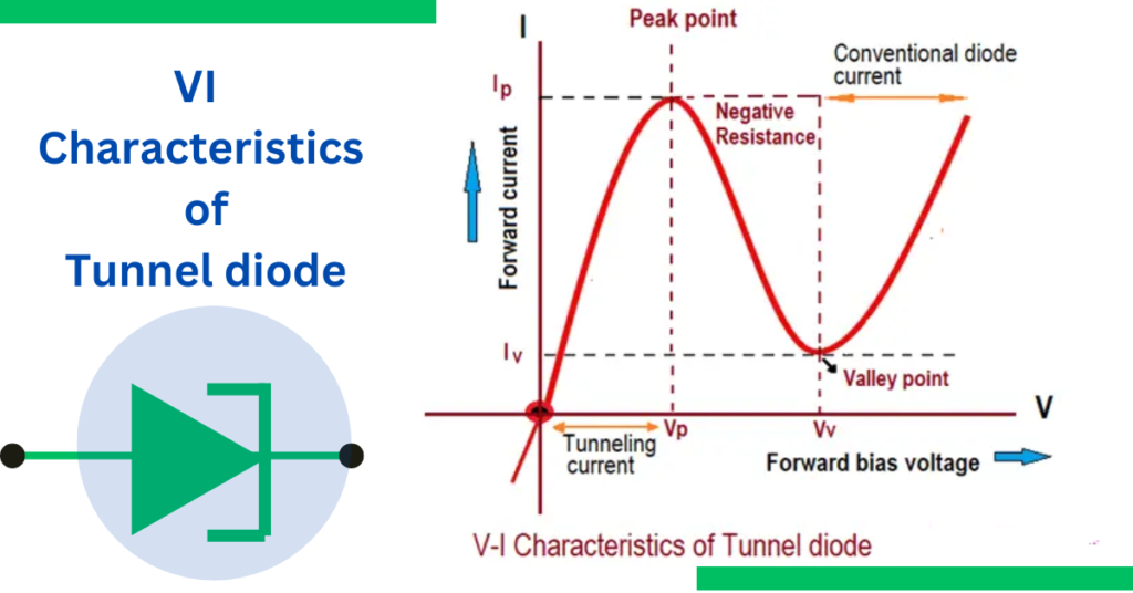
When the band edge of the n-side is aligned with the Fermi level in the p-side, the tunnel current reaches its maximum. The tunnel current decreases as the forward bias increases, and the desired negative conduction region is achieved. It further increases the forward bias, resulting in a normal pn junction current exponentially proportional to the applied voltage. These features can describe the V-I characteristics of the tunnel diode. The negative resistance is commonly utilized to generate oscillation.
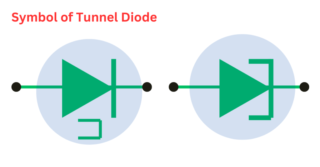
Tunnel Diode Symbol
The symbol for a tunnel diode is depicted below.
Working of Tunnel Diode
Unbiased Tunnel Diode
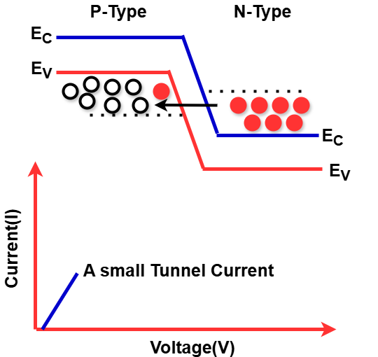
In an unbiased tunnel diode, no external voltage is applied. Due to heavy doping, the conduction band of the n-type semiconductor overlaps with the valence band of the p-type material. As a result, electrons from the n-region and holes from the p-region are at the same energy level and overlap.
At higher temperatures, some electrons from the conduction band of the n-region tunnel into the valence band of the p-region, and holes move in the opposite direction. Since an equal number of electrons and holes move in opposite directions, the net current remains zero.
The probability (P) of a particle crossing the barrier is given by:
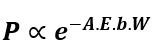
Where:
- P = Probability of tunneling
- W= Barrier width
- E = Barrier energy
Small Voltage Applied to the Tunnel Diode
When a small voltage is applied to the tunnel diode, which is less than the built-in potential of the depletion layer, there is no significant forward current through the junction. However, a small number of electrons from the n-region’s conduction band start tunneling into the p-region’s valence band.
This movement results in a small forward-biased tunnel current. As voltage increases slightly, tunnel current starts flowing through the diode.
Increased Voltage Applied to the Tunnel Diode
With an increase in the applied voltage, more free electrons are generated in the n-region, and more holes appear in the p-region. The overlap between the conduction and valence bands increases, enabling more electrons to tunnel through the barrier.
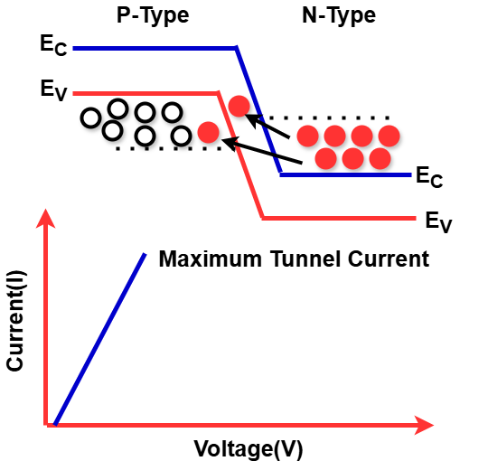
The maximum tunneling current occurs when the energy levels of the n-side conduction band and the p-side valence band become equal. At this point, the peak current flows through the tunnel diode.
Further Increased Voltage Applied to the Tunnel Diode
If the applied voltage continues to increase, the conduction and valence bands slightly misalign, reducing the tunneling probability. However, some overlap still exists, and electrons continue to move from the n-region’s conduction band to the p-region’s valence band.
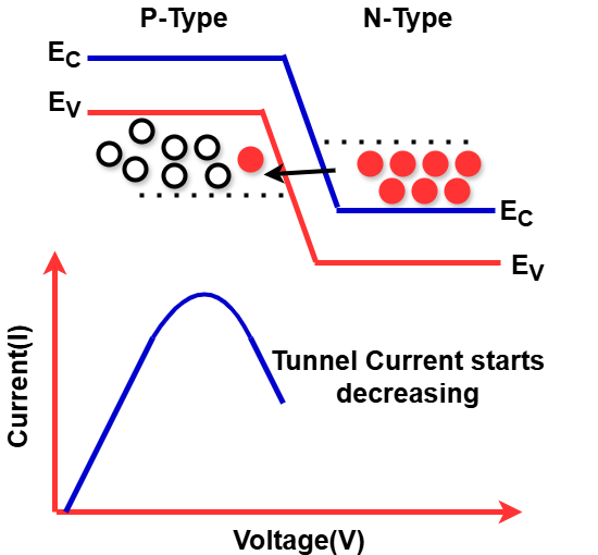
At this stage, the tunnel current starts decreasing, leading to the negative resistance behavior of the tunnel diode.
Largely Increased Voltage Applied to the Tunnel Diode
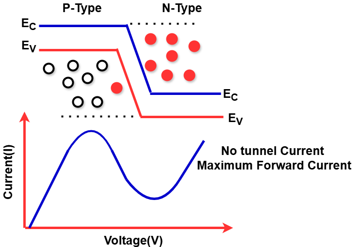
When the applied voltage is increased beyond a certain point, the conduction and valence bands no longer overlap, preventing electron tunneling. At this stage, the tunneling current drops to zero, and the tunnel diode functions like a standard PN junction diode.
If the applied voltage exceeds the built-in potential of the depletion layer, regular forward current starts flowing through the diode. In this condition, as voltage increases, the current initially decreases, leading to a negative resistance region.
Tunnel diodes operating in this negative resistance region are widely used in applications such as amplifiers and oscillators due to their unique high-speed switching properties.
Tunnel Diode Applications
A tunnel diode is a semiconductor diode capable of operating at very high speeds, particularly in the microwave frequency. It derives its unique characteristics from a quantum mechanical effect known as tunneling. Thanks to its negative slope characteristics, it is ideal for use in fast oscillators and receivers. However, its applications are somewhat limited due to its inability to be used in large integrated circuits.
When a voltage is applied, a current begins to flow through it. As the voltage increases, the current also increases. However, once the voltage reaches a certain point, the current suddenly increases again, and the tunnel diode behaves like a normal diode. This unique behavior makes it useful for various special applications, which we’ll explore below.
Oscillator Circuits:
Tunnel diodes are often utilized as high-frequency oscillators due to their rapid transition between high electrical conductivity states. These diodes can generate oscillations as high as 5 GHz; they can even produce oscillations up to 100 GHz in digital circuits.
Used in Microwave Circuits:
Ordinary diode transistors are not suitable for efficient performance in microwave operations. To overcome this limitation, tunnel diodes are utilized in microwave generators and amplifiers. These diodes were previously popularly used in microwave waves and satellite communication equipment. However, in recent times, their usage has declined considerably due to the availability of transistors that operate in this frequency range.
Resistant to Nuclear Radiation:
Tunnel diodes have remarkable resistance to magnetic fields, high temperatures, and radioactivity. This makes them an ideal component for modern military equipment. Additionally, they are used in nuclear magnetic resource machines. However, the most significant application of tunnel diodes is in satellite communication equipment.