In semiconductor physics, the concept of depletion width is central to understanding the behavior of p-n junctions, which are fundamental components of various electronic devices such as diodes, transistors, and solar cells. The depletion region width describes the region around the p-n junction where mobile charge carriers (free electrons and holes) have been swept away, leaving behind a zone of fixed charged ions. This article delves into the definition of depletion width, provides its formula, derives this formula, and presents a solved example to illustrate the concept.
Definition of Depletion Width
In semiconductor physics, particularly in the study of p-n junctions, the depletion width refers to the region where mobile charge carriers (free electrons and holes) have been swept away due to the diffusion across the junction. This leaves behind a zone with only fixed charged ions, creating an electric field. The PN junction width is crucial in defining the electrical behavior of diodes, transistors, and other semiconductor devices.
Depletion Width Formula
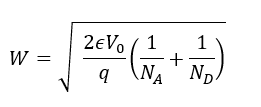
The depletion width (𝑊) in a p-n junction can be expressed by the formula:
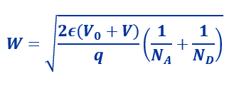
Where:
- ϵ is the permittivity of the semiconductor material,
- 𝑉0 is the built-in potential of the junction,
- 𝑉 is the externally applied voltage (positive for forward bias and negative for reverse bias),
- 𝑞 is the elementary charge (approximately1.6×10−19 Coulombs),
- 𝑁𝐴 and 𝑁𝐷 are the acceptor and donor doping concentrations, respectively.
Depletion Width Formula Derivation
The derivation of the depletion width formula in a semiconductor junction (like a PN junction) involves understanding the behavior of charge carriers and electric fields at the interface between P-type and N-type semiconductors. The depletion region is where mobile charge carriers (electrons and holes) are absent, creating an area dominated by the immobile ionized donor and acceptor impurities. Here’s a step-by-step derivation:
Step 1: Basic Assumptions
- Uniform Doping: Assume the P-type and N-type regions are uniformly doped with acceptor density 𝑁𝐴 and donor density 𝑁𝐷, respectively.
- One-dimensional Analysis: Consider only the one-dimensional case along the x-axis across the PN junction.
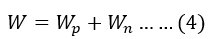
Step 2: Charge Neutrality
The total charge in the depletion region must be zero for overall electrical neutrality: 𝑄𝑝+𝑄𝑛=0 where:
- 𝑄𝑝=−𝑞𝑁𝐴𝑊𝑝 is the charge in the P-type depletion region.
- 𝑄𝑛=𝑞𝑁𝐷𝑊𝑛 is the charge in the N-type depletion region.
- 𝑊𝑝 and 𝑊𝑛 are the widths of the depletion regions in the P-type and N-type materials, respectively.
- 𝑞 is the elementary charge.
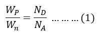
Step 3: Relationship Between Wp and Wn
Using charge neutrality:
𝑁𝐴𝑊𝑝=𝑁𝐷𝑊𝑛
This can be rearranged to relate the widths of the depletion regions:
Step 4: Electric Field and Potential Drop
The electric field 𝐸 reaches its maximum at the metallurgical junction with:
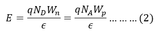
Where 𝜖 is the permittivity of the semiconductor.
By integrating the electric field across the depletion region, the built-in voltage V0 (also called the contact potential) is found:
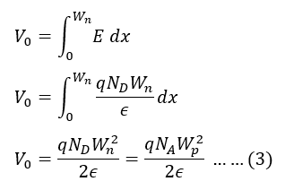
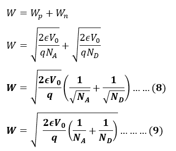
Step 5: Total Depletion Width 𝑊
The total width 𝑊
Using the charge neutrality and the relationship between 𝑊𝑝 and 𝑊𝑛:
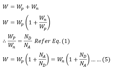
Step 6: Solving for 𝑊
Substitute the expression for 𝑊𝑛 or 𝑊𝑝 from the potential drop:
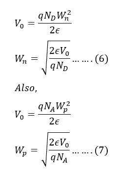
Then, the total depletion width W is given by:
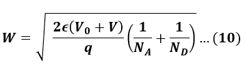
If external voltage (V) is applied to the PN junction and the diode is in reverse bias, the depletion region is,
If external voltage (V) is applied to the PN junction and the diode is in forward bias, the depletion region is,
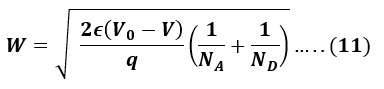
This formula quantifies the width of the depletion region as a function of the doping concentrations, the permittivity of the material, and the built-in voltage across the junction. It’s fundamental in understanding how PN junctions behave under different electrical and environmental conditions.
Solved Problem
A silicon PN junction at room temperature and its width are used as an example to solidify understanding of the theoretical derivation.
Problem-1
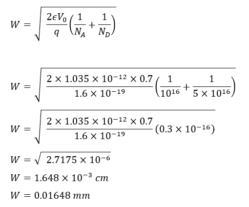
A silicon PN junction at room temperature (300 K) has a uniform acceptor concentration 𝑁𝐴=1016 cm−3 in the P-type region and a donor concentration 𝑁𝐷=5×1016 cm−3 in the N-type region. Assume the built-in potential 𝑉0 is 0.7 V. Calculate the depletion width of this junction.
Constants
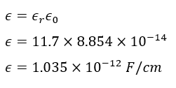
- Elementary charge, 𝑞=1.6×10⁻¹⁹ C
- Relative permittivity of silicon, 𝜖𝑟=11.7
- Permittivity of free space, 𝜖0=8.854×10⁻¹⁴ F/cm
- Permittivity of silicon, 𝜖=𝜖𝑟𝜖0
Solution
Step 1: Calculate the permittivity of silicon
Step 2: Apply the PN Junction width formula
Using the formula:
We substitute the given values:
Problem-2
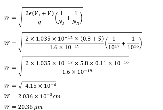
Consider a silicon PN junction with an acceptor concentration 𝑁𝐴=1017 cm−3 in the P-type region and a donor concentration 𝑁𝐷=1016 cm−3 in the N-type region. The built-in potential 𝑉0 is 0.8 V. Calculate the depletion width when a reverse bias of 5 V is applied to the junction.
Constants
- Elementary charge, 𝑞=1.6×10⁻¹⁹ C
- Relative permittivity of silicon, 𝜖𝑟=11.7
- The permittivity of free space, 𝜖0=8.854×10⁻¹⁴ F/cm
Solution
Step 1: Calculate the permittivity of silicon

Step 2: Calculate W
Conclusion
In conclusion, the study of depletion width in PN junctions provides a fundamental insight into the operational principles of semiconductor devices, from defining what depletion width is and why it forms to deriving its quantitative formula and applying this knowledge through solved examples.