Explore the key differences between forward bias and reverse bias in semiconductor diodes and learn how their behavior is illustrated through current-voltage (I-V) characteristics. This guide provides a clear understanding of how diodes operate in different biasing conditions, including the effects of voltage on current flow, the role of the depletion zone, and the phenomenon of diode breakdown. It is perfect for students and electronics enthusiasts seeking a deeper insight into diode functionality.
What is a Semiconductor Diode?
The fundamental structure of a semiconductor diode involves a junction formed from two differently doped semiconductor materials: p-type, which is rich in positive charge carriers (holes), and n-type, which is rich in negative charge carriers (electrons).
When these two semiconductors are joined, they form a p-n junction. At this junction, holes and electrons diffuse into each other’s regions, creating a depletion zone with a built-in electric field that opposes the flow of charge carriers. This physical setup enables the diode’s rectifying behavior under forward bias, where the positive side of the voltage is applied to the p-type material, and the negative side to the n-type, and the depletion zone narrows, allowing current to pass. Conversely, in reverse bias, the depletion zone widens significantly, blocking current flow except in very high voltages, which can lead to breakdown.
The symbol for the p-n junction diode indicates the current direction. Applying an external voltage V can modify the potential barrier.
Semiconductor Diode Symbol
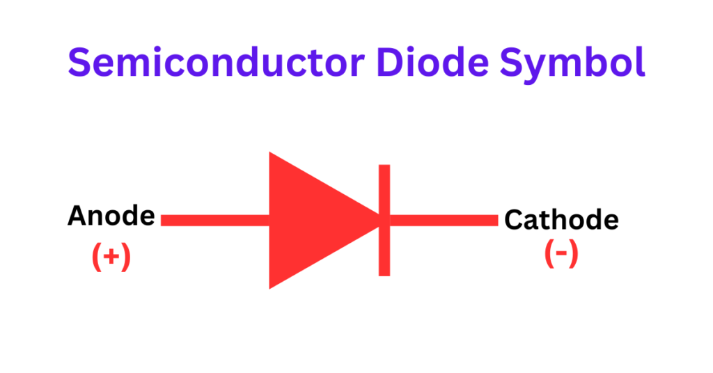
The symbol consists of a triangle pointing towards a line. The triangle represents the anode and the line represents the cathode. The direction of the triangle points from the anode to the cathode, indicating the direction that current can flow through the diode (from anode to cathode under forward-bias conditions).
P-N Junction Diode Under Forward Bias
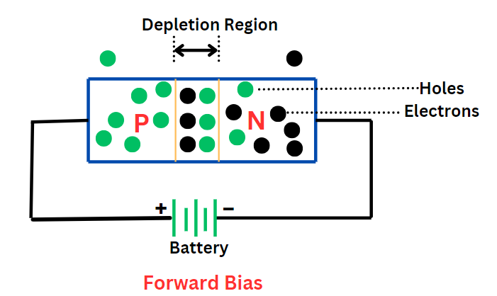
When a p-n junction diode is under forward bias, it operates where the external voltage applied across the diode assists in pushing charge carriers across the junction, thereby facilitating the flow of current through the diode. Here’s how it works step by step:
- P-N Junction Structure: A p-n junction diode is composed of two adjacent types of semiconductor material: p-type, which has an excess of holes (positive charge carriers), and n-type, which has an excess of electrons (negative charge carriers).
- Connecting the Diode: In forward bias, the positive terminal of the voltage source is connected to the p-type side of the diode, and the negative terminal is connected to the n-type side.
- Reduction of Barrier Potential: By applying the external voltage, the built-in potential barrier at the junction, which naturally opposes the movement of electrons from n-type to p-type and holes in the opposite direction, is reduced. This built-in potential is a result of the diffusion of charge carriers across the junction during the manufacturing process, which creates a depletion region where no free charge carriers exist.
- Narrowing the Depletion Zone: The application of forward bias voltage reduces the width of this depletion zone. As the external voltage increases, the barrier becomes thin enough to allow charge carriers to cross the junction more easily.
- Current Flow: Electrons in the n-type region gain enough energy to overcome the reduced barrier and move across to the p-type region, while holes move from the p-type to the n-type region. The actual movement involves electrons flowing into the n-type region from the external circuit and holes flowing into the p-type region, which appears as a current flowing from the p-side to the n-side through the diode.
- Conduction: As more charge carriers are able to cross the junction, the diode conducts current efficiently, essentially acting as a low-resistance path in the circuit in the direction from p-type to n-type semiconductor.
P-N Junction Diode Under Reverse Bias

When a p-n junction diode is under reverse bias, it operates in a condition where the external voltage applied across the diode opposes the flow of charge carriers across the junction, effectively blocking current flow. Here’s how it works step by step:
- P-N Junction Structure: A p-n junction diode is made up of two semiconductor types: p-type, which has an excess of holes (positive charge carriers), and n-type, which has an excess of electrons (negative charge carriers).
- Connecting the Diode: In reverse bias, the positive terminal of the voltage source is connected to the n-type side of the diode, and the negative terminal is connected to the p-type side.
- Increase of Barrier Potential: The external voltage applied enhances the built-in potential barrier at the junction. This potential barrier naturally exists due to the diffusion of charge carriers that occurred when the junction was formed, creating a depletion region where there are no free charge carriers.
- Widening the Depletion Zone: Applying reverse bias voltage widens the depletion zone. The widened depletion zone increases the barrier that opposes the flow of electrons from the n-type to the p-type and holes in the opposite direction.
- Blocking of Current Flow: With the barrier increased, the flow of charge carriers is minimized. Very little current, known as the reverse saturation current, flows due to the thermal generation of electron-hole pairs within the depletion region. This current is typically very small, on the order of nanoamperes (nA).
- High Resistance Path: The diode in reverse bias acts as a high-resistance path in the circuit, effectively blocking any significant flow of current.
- Breakdown Condition: If the reverse bias voltage is increased beyond a certain threshold, known as the breakdown voltage, the diode can undergo a breakdown (either through avalanche or Zener breakdown depending on the type of diode), where it starts to conduct current in reverse. This is often used deliberately in certain types of diodes like Zener diodes for voltage regulation purposes.
Semiconductor Diode Characteristics
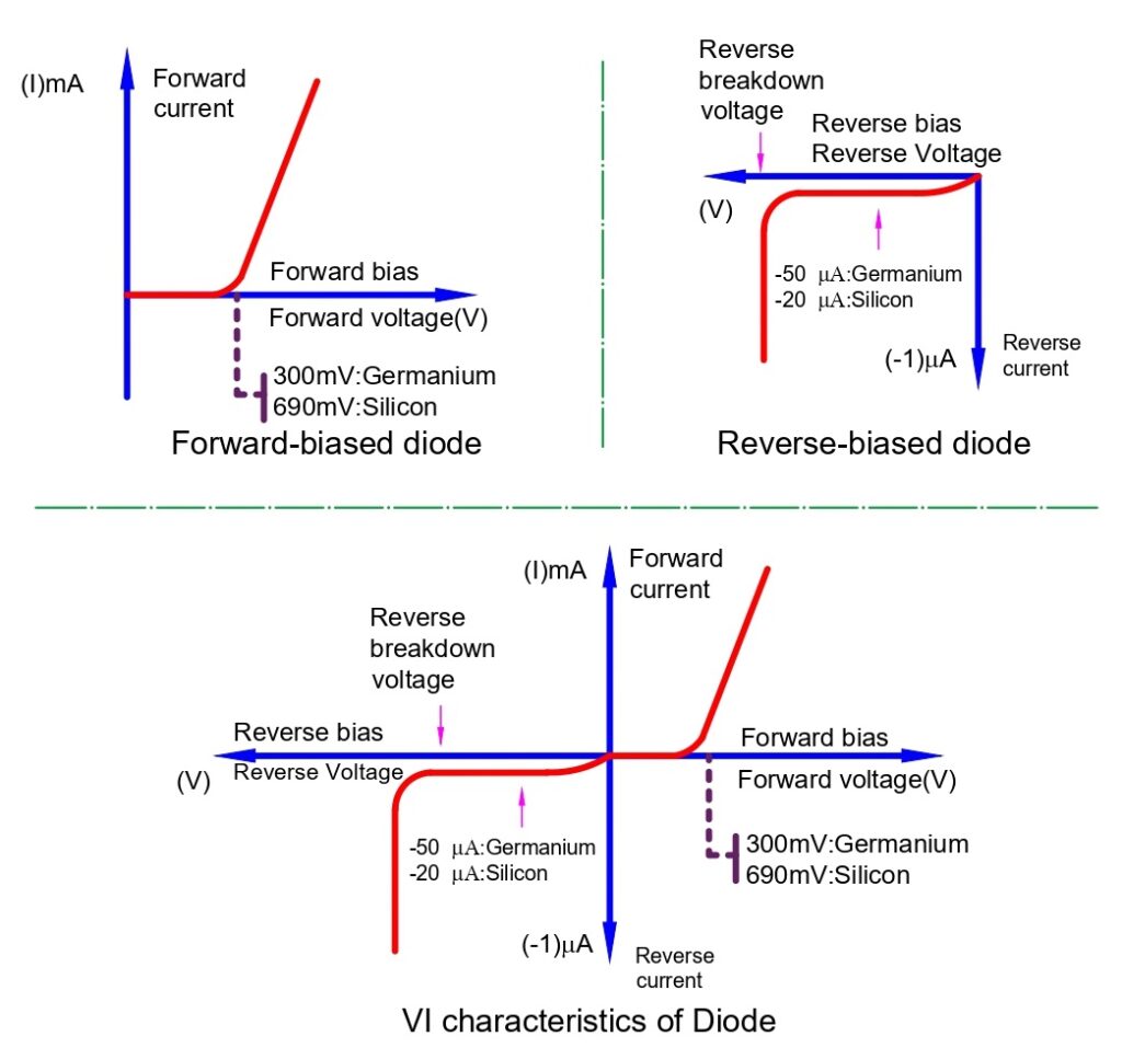
The characteristics of a semiconductor diode can be understood by studying its behavior in a circuit, particularly through its current-voltage (I-V) relationship. This relationship is typically illustrated in a graph that plots the current flowing through the diode against the applied voltage. The characteristics can be broadly divided into three main regions: forward bias, reverse bias, and breakdown. Here’s a detailed look at each:
1. Forward Bias Region
- Voltage Application: In this mode, the positive terminal of the voltage source is connected to the p-type material and the negative to the n-type material.
- Current Flow: Initially, as the forward voltage is applied, the current remains very small until the diode reaches what is known as the threshold or cut-in voltage (typically about 0.7 volts for silicon diodes and 0.3 volts for germanium diodes).
- After Threshold: Once the threshold voltage is exceeded, the current increases exponentially with a slight increase in voltage. This is due to the significant reduction in the width of the depletion zone, allowing a large number of charge carriers to cross the junction.
- Characteristic Curve: The forward characteristic curve is steep, indicating a high sensitivity of current to changes in voltage beyond the threshold.
2. Reverse Bias Region
- Voltage Application: Here, the polarity is reversed, with the positive terminal connected to the n-type material and the negative to the p-type.
- Current Behavior: The current remains very low, typically in the range of nanoamperes. This current, known as the reverse saturation current, is due to minority carriers and is relatively constant with increasing reverse voltage.
- Depletion Zone: The depletion zone widens in reverse bias, enhancing the junction’s resistance to current flow.
- Characteristic Curve: The reverse bias curve is relatively flat, showing very little current flow up to a critical point.
3. Breakdown Region
- High Reverse Voltage: When the reverse voltage applied to the diode exceeds a certain critical level, the diode experiences a breakdown characterized by a sudden increase in current.
- Breakdown Mechanisms: There are two primary mechanisms:
- Avalanche Breakdown: Occurs when the reverse-biased voltage causes the minority carriers to accelerate to the extent that they generate additional charge carriers through collisions, leading to a multiplication of carriers.
- Zener Breakdown: This happens at lower voltages compared to an avalanche and is caused by a quantum mechanical effect called tunneling, where electrons tunnel through the potential barrier at the junction.