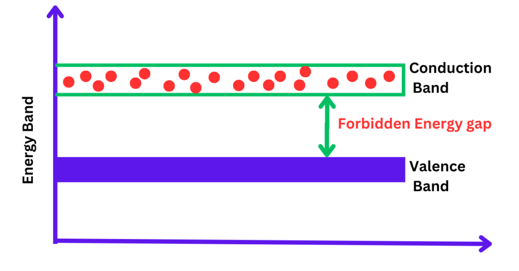
Definition: The forbidden energy gap, also known as the band gap, is the range of energy between the valence band and the conduction band in a solid where no electron states can exist. It is the energy difference that electrons must overcome to move from the valence band to the conduction band, which is essential in determining the electrical conductivity of materials.
Forbidden Energy Gap for Germanium Semiconductor
The forbidden energy gap, or band gap, for a germanium semiconductor, is approximately 0.66 eV (electron volts) at room temperature (around 300 K).
What is the value of the forbidden energy gap for silicon at room temperature?
The forbidden energy gap, or band gap, for silicon at room temperature (approximately 300 K) is about 1.12 eV (electron volts).
Forbidden Energy Gap for Insulator
In an insulator, the forbidden energy gap (band gap) between the valence band and the conduction band is typically on the order of 5 eV (electron volts) or more. This large band gap prevents electrons from easily moving from the valence band to the conduction band, resulting in poor electrical conductivity.
Since the forbidden energy gap (band gap) for a diamond is approximately 6 eV, a diamond is classified as an insulator. This large band gap means that electrons cannot easily move from the valence band to the conduction band, making diamond an excellent electrical insulator.
The forbidden energy gap is large in insulators. Insulators have a large band gap, typically on the order of 5 eV or more, which prevents electrons from easily moving from the valence band to the conduction band, resulting in poor electrical conductivity. Examples of materials with large band gaps include diamond and various ceramics.
Forbidden Energy Gap of Gallium Arsenide (GaAs)
The forbidden energy gap (band gap) of Gallium Arsenide (GaAs) is approximately 1.43 eV (electron volts) at room temperature. This direct band gap makes GaAs an excellent material for optoelectronic applications such as LEDs, laser diodes, and high-efficiency solar cells.
Does Forbidden Energy Gap Applicable for Conductor?
In conductors, the concept of a forbidden energy gap (band gap) is not applicable in the same way as it is for semiconductors and insulators. This is because:
- Metals (Conductors): In conductors, the valence band and the conduction band overlap, or the conduction band is partially filled with electrons. This means there is no significant energy gap preventing electrons from moving and conducting electricity.
Thus, conductors have either zero band gap or a very small overlap, allowing free movement of electrons and resulting in high electrical conductivity.
Effect of Temperature on Forbidden Gap of Semiconductor
As the temperature of a semiconductor falls, the forbidden energy gap (band gap) typically increases. This occurs because:
- Lattice Vibrations Decrease: At lower temperatures, the vibrations of the atomic lattice decrease. These vibrations can affect the energy levels of the electrons, and with fewer vibrations, the energy levels stabilize, causing the band gap to widen.
- Thermal Expansion Reduces: As temperature decreases, the thermal expansion of the semiconductor material also reduces. This change can lead to a slight increase in the band gap because the distance between atoms in the lattice becomes more fixed and stable.
This increase in the band gap with decreasing temperature affects the electrical properties of the semiconductor, often leading to reduced intrinsic carrier concentration and changes in conductivity.
How does the Forbidden Energy gap occur?
The forbidden energy gap, or band gap, occurs due to the quantum mechanical behavior of electrons in a solid and the periodic arrangement of atoms in a crystal lattice. When atoms come together, their discrete energy levels split into energy bands. The valence band is filled with electrons, while the conduction band is higher in energy and typically empty. The band gap is the energy range between these two bands where no electron states can exist, caused by the periodic potential of the lattice. This gap determines the electrical and optical properties of the material, with conductors having no gap, and semiconductors and insulators having significant gaps.
Conclusion
In conclusion, the forbidden energy gap, is a fundamental concept in solid-state physics that defines the energy range between the valence band and the conduction band where no electron states can exist. This gap arises from the quantum mechanical interactions and the periodic potential within a crystalline lattice. The size of the band gap plays a crucial role in determining a material’s electrical and optical properties, distinguishing conductors (no gap), semiconductors (small gap), and insulators (large gap). Understanding the band gap is essential for designing and utilizing materials in various electronic and optoelectronic applications.