The VI characteristics of a PN junction diode describe the relationship between the voltage applied across the diode and the current flowing through it under forward and reverse bias conditions.
A PN junction diode is a two-terminal semiconductor device formed by joining p-type and n-type semiconductor materials. Its electrical behavior depends on the applied voltage and the resulting changes in the depletion region at the junction.
- Forward bias: The diode allows current to flow when the applied forward voltage is sufficient to overcome the junction potential barrier.
- Reverse bias: The diode permits only a very small leakage current under normal operating conditions, effectively preventing current flow.
- Depletion region: The region around the junction acts as a barrier to charge carrier movement. Its width changes with the applied voltage, influencing the diode’s current-voltage behavior.
The VI characteristic curve helps explain how a diode behaves under different operating conditions and identifies important parameters such as the cut-in voltage, reverse saturation current, and breakdown voltage.
Formation of a PN Junction
A PN junction is formed when p-type and n-type regions are created within the same semiconductor crystal. For example, a silicon crystal can be doped with a trivalent impurity to form a p-type region and with a pentavalent impurity to form an n-type region. The interface between these two regions is known as the PN junction.
When the junction is formed, electrons from the n-type region diffuse into the p-type region, while holes from the p-type region diffuse into the n-type region. This movement occurs because of the difference in charge carrier concentrations and produces diffusion current.
The formation of a PN junction involves the following processes:
- Recombination of charge carriers: Electrons crossing into the p-type region recombine with holes, while holes entering the n-type region recombine with electrons near the junction.
- Formation of the depletion region: Recombination leaves behind immobile, ionized donor atoms on the n-side and ionized acceptor atoms on the p-side. These fixed charges create a region depleted of mobile charge carriers.
- Development of the electric field: The fixed positive and negative charges establish an electric field across the depletion region, creating a potential barrier that opposes further diffusion.
- Establishment of equilibrium: The electric field causes charge carriers to drift in the opposite direction to diffusion. At thermal equilibrium, the drift current and diffusion current balance each other, resulting in zero net current through the unbiased junction.
Forward Bias
Forward bias occurs when the p-type region of a PN junction diode is connected to the positive terminal of a battery and the n-type region is connected to its negative terminal.
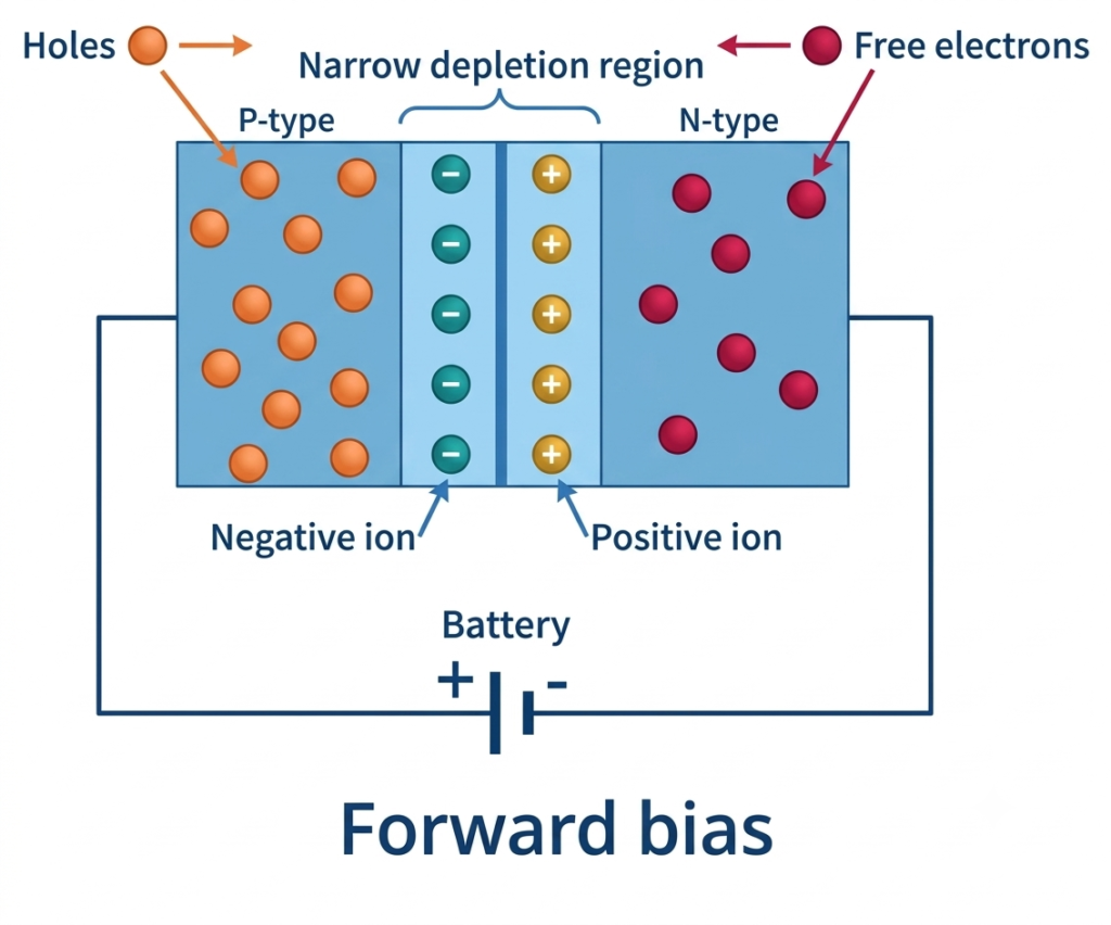
In this condition, the external voltage reduces the built-in potential barrier at the junction, allowing charge carriers to cross the depletion region more easily. Consequently, the depletion region becomes narrower, and the diode’s resistance decreases.
As the applied forward voltage increases, the current through the diode rises rapidly. For a silicon diode, the forward current becomes significant at approximately 0.7 V, whereas for a germanium diode, it is typically around 0.3 V. These values are approximate and depend on the diode’s characteristics and operating conditions.
Reverse Bias
Reverse bias occurs when the n-type region of a PN junction diode is connected to the positive terminal of a battery and the p-type region is connected to the negative terminal.
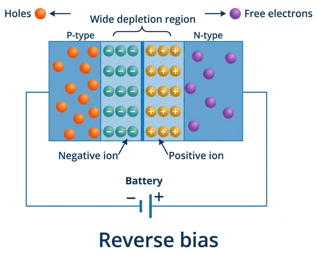
Under this condition, the applied electric field reinforces the built-in electric field across the junction, increasing the potential barrier. Consequently, the depletion region widens, making it more difficult for majority charge carriers to cross the junction. The diode therefore exhibits very high resistance, allowing only a small reverse leakage current to flow.
When the reverse voltage increases, the electric field across the depletion region becomes stronger. Once the applied voltage reaches the diode’s breakdown voltage, the reverse current increases sharply. This phenomenon is known as reverse breakdown. The current must be limited externally to prevent damage to an ordinary diode, unless the device is specifically designed to operate in the breakdown region.
V-I Characteristics of a PN Junction Diode
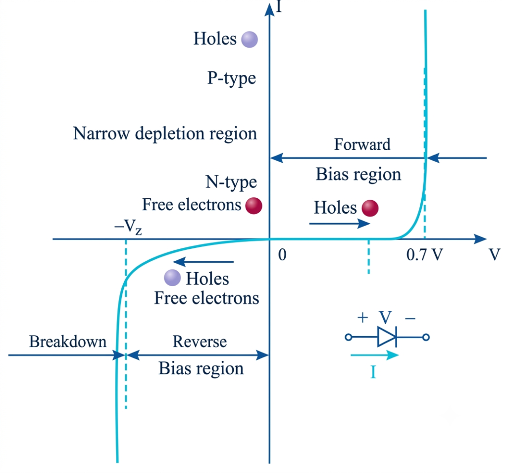
The voltage-current (V-I) characteristic curve of a PN junction diode shows the relationship between the applied voltage across the diode and the resulting current under forward and reverse bias conditions. It illustrates the diode’s nonlinear behavior and identifies its three main operating regions: forward bias, reverse bias, and breakdown.
Forward-Bias Region
In the forward-bias condition, the p-side of a PN junction diode is connected to the positive terminal of the voltage supply, while the n-side is connected to the negative terminal. This represents the forward characteristics of the diode when the applied voltage is positive .
In this condition, the applied voltage reduces the junction’s potential barrier and narrows the depletion region, allowing charge carriers to cross the junction more easily. At low forward voltages, the current remains relatively small because the potential barrier still restricts the movement of charge carriers. As the applied voltage increases and approaches the cut-in voltage, the current begins to rise significantly. Beyond this point, even a small increase in forward voltage produces a sharp increase in current.
The voltage at which the forward current starts increasing rapidly is called the cut-in voltage, knee voltage, or threshold voltage, denoted by .
The typical cut-in voltages are:
- Silicon diode:
- Germanium diode:
These values are approximate and may vary with the diode’s operating current, temperature, and construction.
Reverse-Bias Region
In the reverse-bias condition, the p-side of a PN junction diode is connected to the negative terminal of the voltage supply, while the n-side is connected to the positive terminal. This represents the reverse characteristics of the diode when the applied voltage is negative .
Under this condition, the applied voltage increases the potential barrier and widens the depletion region, restricting the movement of majority charge carriers across the junction. As a result, the diode offers very high resistance, and only a very small reverse saturation current flows. This current is mainly caused by thermally generated minority charge carriers and remains nearly constant over much of the reverse-bias region.
The reverse current is practically negligible under normal operating conditions. However, when the reverse voltage reaches the breakdown voltage , the current increases sharply. In a conventional diode, this current must be limited to a safe value to prevent damage.
Cut-in voltage
Also known as the knee voltage or threshold voltage, the cut-in voltage is the approximate forward voltage at which the diode current begins to increase significantly. Its typical value is around 0.3 V for germanium diodes and 0.7 V for silicon diodes. Beyond this region, a small increase in forward voltage produces a substantial increase in current.
Breakdown Region
A PN junction diode enters the breakdown region when the reverse voltage reaches its specified breakdown voltage . In this region, even a small increase in reverse voltage causes a sharp rise in reverse current due to the Zener or avalanche breakdown mechanism.
The breakdown voltage depends on the diode’s construction, doping concentration, and operating conditions. Beyond this point, the diode’s reverse current can increase significantly, so an external current-limiting mechanism is necessary to prevent excessive current, overheating, and damage.
A conventional PN junction diode should not be operated beyond its rated limits unless the circuit provides adequate current protection. However, diodes specifically designed for breakdown operation, such as Zener diodes, can operate safely in this region when the reverse current and power dissipation remain within their specified ratings.
The V-I characteristic curve demonstrates the nonlinear nature of a PN junction diode. Under forward bias, the diode conducts significant current after the cut-in region, whereas under reverse bias, it blocks most current until breakdown occurs. These characteristics make the diode useful in rectifiers, electronic switching circuits, and voltage-regulation applications.
Conclusion
The V-I characteristics of a PN junction diode explain how the diode current varies with the applied voltage under forward and reverse bias conditions. In forward bias, the current increases rapidly after the cut-in voltage, typically 0.7 V for silicon and 0.3 V for germanium diodes. In reverse bias, only a small leakage current flows until the breakdown voltage is reached, beyond which the reverse current rises sharply. Understanding these characteristics is essential for selecting and using diodes in rectifiers, switching circuits, and voltage-regulation applications.
Read Next: