Definition: The depletion region, also known as the depletion layer, is a specific area within a P-N junction diode. In this area, there are no mobile charge carriers present. The depletion layer acts as a barrier that opposes the flow of electrons from the n-side and holes from the p-side.
A PN junction is formed when a p-type semiconductor, which has an abundance of holes (positive charge carriers), is fused with an n-type semiconductor, which has an excess of electrons (negative charge carriers). This junction is pivotal in the operation of devices such as diodes, transistors, and solar cells.
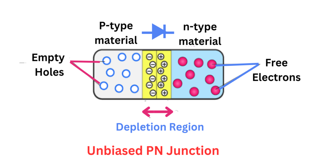
What is the Depletion Region in PN Junction?
The depletion region in a PN junction is a zone where the mobile charge carriers (holes in the p-type and electrons in the n-type) have diffused across the junction and recombined, leaving behind a zone depleted of free charge carriers. This region is thus characterized by the presence of ionized donor and acceptor impurities, which create an electric field.
Formation of the Depletion Region
The formation of the depletion region occurs naturally when the PN junction is created. Electrons from the n-type material diffuse into the p-type material and recombine with holes near the junction. Similarly, holes from the p-type diffuse into the n-type and recombine with electrons. As electrons and holes move across the junction and recombine, they leave behind their respective ionized impurities: positively charged donor ions in the n-type region and negatively charged acceptor ions in the p-type region. This leads to the formation of an electric field within the depletion region, acting as a barrier that prevents further movement of holes and electrons across the junction.
Effects of Electrical Biasing on Depletion Region
Electrical biasing of a PN junction refers to the application of an external voltage across the junction. This external voltage can either be forward bias or reverse bias, significantly impacting the depletion region’s properties.
Forward Bias
In forward bias, the external voltage is applied to reduce the potential barrier created by the electric field in the depletion region. Specifically, the positive terminal is connected to the p-type material, and the negative terminal is connected to the n-type material. This alignment reduces the width of the depletion region because it pushes the holes and electrons toward the junction, encouraging recombination. As a result, the conductivity of the junction increases, allowing a higher current to flow through the device.
Reverse Bias
Conversely, when the PN junction is reverse-biased, the external voltage increases the potential barrier of the electric field. In this setup, the positive terminal is connected to the n-type material and the negative to the p-type material. This alignment widens the depletion region as the electric field forces the carriers away from the junction, thus reducing the movement of charge carriers across the junction. Consequently, the conductivity decreases, and very little current flows through the junction, except for a minor leakage current.
Conclusion
The depletion region is a critical concept of PN junctions that states the electrical characteristics under different conditions. By understanding the behavior of this region under forward and reverse bias, you can better design and optimize semiconductor devices for various applications in electronics and energy solutions. Understanding the depletion region helps in the theoretical study of semiconductor physics and enhances the practical application of these principles in developing electronic and photonic devices.