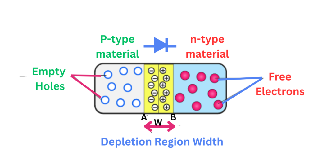
The depletion region width of the PN junction is significantly influenced by the doping concentration of the semiconductor materials used in the PN junction. The doping level determines the concentration of charge carriers in the material, affecting the depletion layer’s physical properties.
Effect of Doping Concentration on Depletion Region Width
We will discuss how doping concentration affects the depletion region width of the PN junction.
Heavily Doped Diodes
In a heavily doped diode, both the p-type and n-type materials have a high concentration of impurities. This high concentration of impurities results in many charge carriers (holes in the p-type and electrons in the n-type). When these charge carriers recombine across the junction, they form a depletion region where the mobile carriers have been used up. However, because the concentration of impurities is high, the electric field established across the depletion region is very strong. Still, it doesn’t need to extend very far to balance the junction voltage. Therefore, the depletion layer in a heavily doped diode is narrower.
Lightly Doped Diodes
Conversely, in a lightly doped diode, the concentration of impurities, and thus charge carriers, is lower. This lower density of charge carriers means that more volume is needed to achieve the same recombination as in a heavily doped diode. Therefore, the depletion region spreads more widely to cover a larger area. This leads to a wider depletion layer because it takes a larger spatial extension of the depletion region to maintain electrical neutrality and to establish the junction voltage.
Summary
In summary, the width of the depletion layer in a diode varies inversely with the doping concentration:
- Heavily Doped Diodes: Have a narrow depletion layer due to the high concentration of charge carriers and the strong resultant electric field across a small region.
- Lightly Doped Diodes: Have a wider depletion layer as the lower concentration of carriers necessitates a broader area to maintain electrical neutrality and to balance the junction voltage.
This understanding is crucial in the design and application of semiconductor devices, as the depletion region width directly affects the diode’s behavior under different operating conditions.