Definition: The potential barrier in the PN -junction diode is the barrier that acts as an obstruction for the charge carrier to cross the region. This barrier requires additional force to overcome and is known as the potential barrier.
How is a Potential Barrier Established?
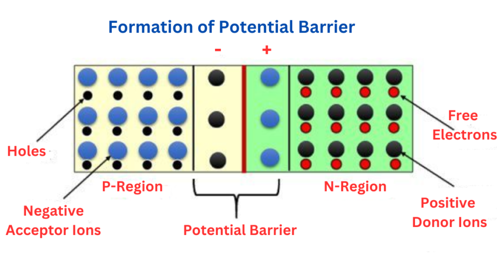
The potential barrier in a PN junction diode is a fundamental phenomenon that occurs when a P-type semiconductor is joined with an N-type semiconductor. This process involves several steps and is crucial for the functioning of diodes in electronic circuits. Here’s a step-by-step breakdown:
1. Contact between P-type and N-type Semiconductors
- P-type Semiconductor: Contains an abundance of holes (positive charge carriers).
- N-type Semiconductor: Contains an abundance of electrons (negative charge carriers).
When these two materials are brought into contact, the interface they create is the PN junction.
2. Diffusion of Charge Carriers
- Electrons Diffusion: Electrons in the N-type region (where they are the majority carriers) begin to diffuse into the P-type region, where they are minority carriers.
- Holes Diffusion: Similarly, holes in the P-type region (majority carriers) diffuse towards the N-type region.
This diffusion process is driven by the concentration gradient of the charge carriers; it continues until an equilibrium is reached.
3. Recombination of Charge Carriers
- Recombination Process: As electrons move from the N-type to the P-type region, they encounter and recombine with holes. This recombination results in a region around the PN junction that becomes depleted of free charge carriers (both electrons and holes).
4. Formation of the Depletion Region
- Depletion of Carriers: The area where the electrons and holes have recombined is now depleted of free charge carriers and is aptly named the depletion region.
- Ionized Impurities: The recombination leaves behind ionized donor atoms (positively charged) in the N-type region and ionized acceptor atoms (negatively charged) in the P-type region.
5. Development of Electric Field
- Built-in Electric Field: The presence of ionized donors and acceptors at the junction creates a built-in electric field. This electric field is directed from the N-type side (positive ions) to the P-type side (negative ions).
- Potential Gradient: This electric field establishes a potential gradient across the junction.
6. Establishment of Potential Barrier
- Potential Barrier: The electric field opposes further diffusion of electrons from the N-side to the P-side and holes from the P-side to the N-side. This opposing force establishes the potential barrier.
- Barrier Potential Value: The value of this potential barrier is typically in the range of 0.3 to 0.7 volts, depending on the materials used in the diode.
7. Stabilization
- Equilibrium Condition: The potential barrier eventually balances out the tendency of electrons and holes to diffuse due to concentration gradients. This stabilization occurs at a point where the electrical force provided by the built-in potential exactly counters the diffusion force.