Explore the key concepts of diode junction capacitance, including its types—diffusion, and transition capacitance—and the mathematical formulas used to calculate them. This post delves into how these capacitances form and their impact on diode performance in various electronic applications.
In semiconductor electronics, diodes play a critical role in controlling the flow of electrical current. A fundamental but often overlooked characteristic of diodes is their junction capacitance. This capacitance arises from the structure of the diode itself and affects its performance in various applications, especially in high-frequency circuits. In this article, we will explore what diode junction capacitance is, its types, and the formulas used to calculate it.
What is Diode Junction Capacitance?
Diode junction capacitance is the electrical capacitance created by the depletion region at the p-n junction of a semiconductor diode. When a diode is reverse-biased, the depletion region widens, and the capacitance decreases. Conversely, the depletion region narrows in forward bias and the capacitance increases. This capacitance is intrinsic to the diode’s physical structure and materials.
Types of Diode Junction Capacitance
There are two primary types of junction capacitance in diodes:
- Diffusion Capacitance(Cd)
- Transition Capacatitance(Ct)
Diffusion Capacitance (Cd)
This type of capacitance is significant in forward-biased conditions. It arises due to the charge carriers (holes and electrons) accumulating on either side of the junction. Diffusion capacitance is typically much larger than other capacitance due to the higher mobility and density of charge carriers in this state.
The diffusion capacitance arises due to this storage and eventual recombination of excess carriers. Essentially, this process can be likened to the charging and discharging of a capacitor. When the forward voltage is applied, the diode “charges up” with excess carriers. When the voltage is reduced or removed, these carriers “discharge” by recombining.
Diffusion capacitance is significantly larger than the depletion (or transition) capacitance in forward bias because it involves the active participation of carriers in the conduction process. This large capacitance is crucial in circuits where diodes are subjected to alternating currents (AC), as it impacts the diode’s frequency response and can lead to increased power consumption and heat generation.
Transition Capacitance (Ct):
It is also known as depletion capacitance. It dominates in reverse-biased conditions. It is associated with the charge storage in the depletion zone that forms at the junction. This capacitance decreases as the reverse bias voltage increases, widening the depletion zone and reducing the ability to store charge.
The formation of transition capacitance can be likened to a parallel plate capacitor. The depletion region acts as the dielectric (insulator) between two plates, which are the edges of the mobile charge regions in the p-type and n-type materials. Just as a capacitor stores energy in the form of an electric field between its plates, the diode stores charge across the depletion region.
Formulas for Calculating Junction Capacitance
Diffusion Capacitance (Cd)
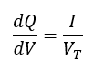
The diffusion capacitance in forward bias can be estimated using the formula:
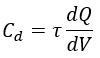
Where:
- τ is the carrier lifetime,
- dQ/dV represents the change in charge with respect to the change in voltage.
Solved Problem on Diffusion Capacitance:
Suppose we have a silicon p-n junction diode with the following parameters:
- Minority carrier lifetime (τ) = 1 microsecond (1×10⁻⁶ seconds),
- Diode current I = 10 mA when forward-biased at 0.7 V,
- Thermal voltage (VT) at room temperature (approximately 26 mV).
Calculate the diffusion capacitance Cd of the diode when it is forward-biased at 0.7 V.
Solution:
1. Calculate dQ/dV
Given that I=10 mA, and using the diode equation, we know:
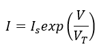
Where V is the forward-bias voltage, and VT is the thermal voltage.
To find dQ/dV, we first recognize that Q=I×t and differentiate I with respect to V:
This is because:
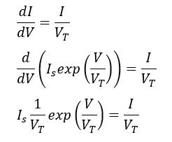
Thus:
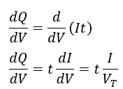
Since we’re looking at a static scenario where time does not extend beyond the characteristic time scales of carrier transit and recombination:
2. Substitute Values to Calculate Cd
Substituting the values, we have:
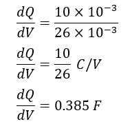
Now calculate Cd:
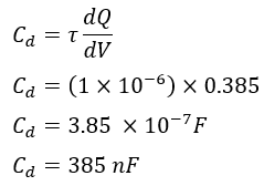
Conclusion: The diode’s diffusion capacitance Cd , when forward-biased at 0.7 V, is approximately 385 nF. This value indicates significant storage of charge due to carrier diffusion under forward bias conditions, which impacts the diode’s performance in circuits, especially at high frequencies.
Transition Capacitance (Ct)
The formula for calculating the transition or depletion capacitance of a diode is given by:

Where:
- ϵ is the permittivity of the semiconductor material,
- A is the cross-sectional area of the junction,
- W is the width of the depletion region.
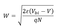
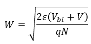
The width of the depletion region W can be calculated as:
Where:
- Vbi is the built-in voltage of the diode,
- V is the applied reverse-bias voltage,
- q is the charge of an electron,
- N is the doping concentration of the semiconductor.
Solved Problem on Transition Capacitance:
Problem Statement:
- Permittivity of silicon (ϵ) = 11.7×ϵ0 (where ϵ0 = 8.85×10⁻¹² F/m is the permittivity of free space),
- Area of the junction (A) = 1 mm² = 1×10⁻⁶ m²,
- Built-in voltage (Vbi) = 0.7 V,
- Applied reverse-bias voltage (V) = 5 V,
- Uniform doping concentration on both sides (N) = 1×1016 cm⁻³.
Calculate the transition capacitance Ct of the diode when it is reverse-biased at 5 V.
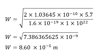
Solution:
1. Convert Units and Calculate Permittivity
First, convert the doping concentration from cm⁻³ to m⁻³:
N=1 x1016 cm-3 = 1 X 10²² m-3
Calculate the permittivity of silicon:
ϵ=11.7×8.85×10−12 F/m
ϵ =1.03645×10⁻¹⁰ F/m
2. Calculate the Width of the Depletion Region W
Using the formula for the width of the depletion region:
Where:
- q is the elementary charge (1.6×10⁻¹⁹ C),
- Vbi + V = 0.7 V + 5 V = 5.7 V.
Plugging in the values:
3. Calculate the Transition Capacitance(Ct)
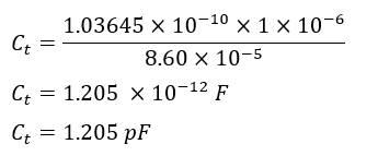
Conclusion: The transition capacitance Ct of the diode when reverse-biased at 5 V is approximately 1.205 pF. This value indicates the diode’s ability to store charge in the depletion region under reverse bias conditions, which is critical for understanding its performance in high-frequency and switching applications.
Importance of Junction Capacitance in Circuit Design
Understanding and calculating the junction capacitance of diodes is crucial for designing effective electronic circuits, particularly in high-frequency applications such as RF communications and fast-switching circuits. The capacitance affects the speed at which a diode can turn on and off and influences the bandwidth and response time of the circuit.
Conclusion
Diode junction capacitance is a key parameter that can significantly influence the performance and functionality of electronic circuits. By understanding its types and utilizing the correct formulas for calculation, engineers can design more efficient and responsive devices. Whether in power rectification, signal modulation, or frequency tuning, junction capacitance is fundamentally important in the practical application of semiconductor diodes.