A PN junction is formed by joining P-type and N-type semiconductor regions within a single semiconductor crystal. The junction creates the basic structure of a semiconductor diode, which allows current to flow more easily in one direction than the other.
Formation of a PN Junction in Semiconductor Materials
PN junction theory describes the electrical behavior that occurs when P-type and N-type semiconductor regions are joined to form a PN junction. This junction is the fundamental structure of a semiconductor diode, whose current flow depends on the polarity of the applied voltage.
The following PN junction diagram illustrates the P-type and N-type semiconductor regions and the depletion layer formed at their junction.
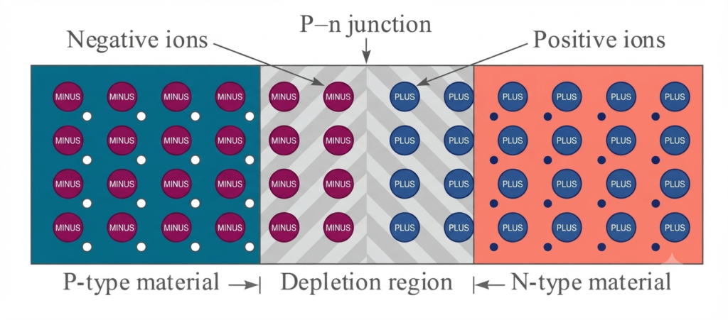
Pure silicon can be converted into N-type or P-type semiconductor material by adding suitable impurities, a process known as doping. Adding a donor impurity such as antimony produces N-type silicon, in which electrons are the majority charge carriers. Similarly, adding an acceptor impurity such as boron produces P-type silicon, in which holes are the majority charge carriers.
Although these two semiconductor materials have different majority charge carriers, each region remains electrically neutral overall. In N-type material, the negative charge of the free electrons is balanced by positively charged ionized donor atoms. In P-type material, the positive charge of the holes is balanced by negatively charged ionized acceptor atoms.
When P-type and N-type regions are formed next to each other in the same semiconductor crystal, electrons and holes begin to diffuse across the junction because of their concentration differences. They recombine near the boundary, leaving behind fixed ions and forming a region depleted of mobile charge carriers. This region is called the depletion region.
The depletion region establishes an internal electric field that affects the movement of charge carriers. When an external voltage is applied, the junction responds differently depending on the biasing condition. Under forward bias, current can flow readily once the applied voltage sufficiently reduces the junction barrier. Under reverse bias, the barrier generally increases, allowing only a small leakage current until breakdown conditions are reached.
These processes form the basis of PN junction theory and explain the rectifying behavior of semiconductor diodes.
Charge Carrier Movement at a PN Junction
When P-type and N-type semiconductor regions are brought into contact, electrons and holes begin moving across the junction due to the difference in their concentrations on either side.
Electrons are more concentrated in the N-type region, so some diffuse into the P-type region, where they recombine with holes. Similarly, holes diffuse from the P-type region into the N-type region and recombine with electrons.
As electrons leave the N-type region, positively charged donor ions remain near the junction. On the P-type side, the recombination of holes leaves negatively charged acceptor ions. These ions are fixed within the semiconductor crystal and cannot move freely.
The accumulation of fixed ions creates a region around the junction with very few mobile charge carriers. This region is called the depletion region. The electric field established within it opposes further diffusion of electrons and holes.
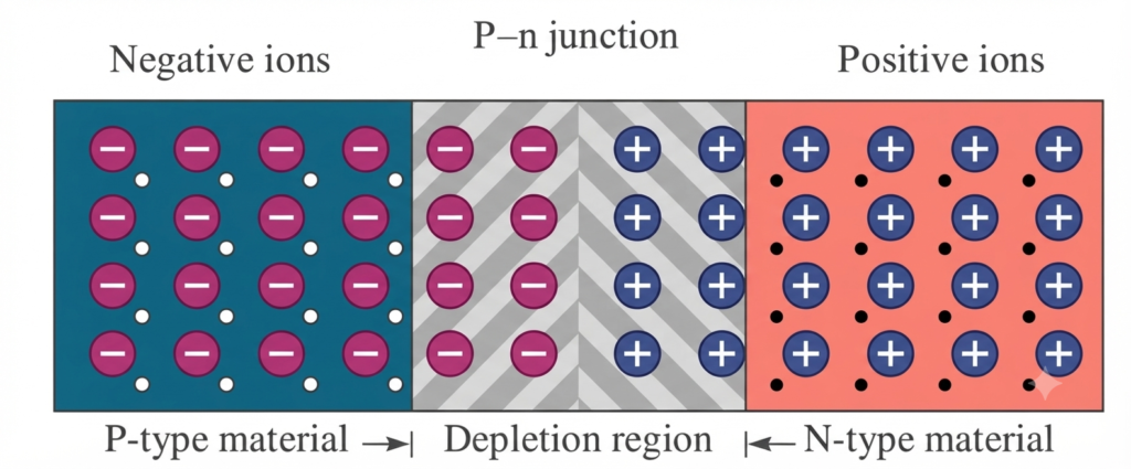
Eventually, the junction reaches equilibrium, where the diffusion of charge carriers is balanced by the opposing drift caused by the internal electric field. The two types of charge carriers do not become uniformly distributed across the junction; instead, a depletion region and a built-in potential barrier are established.
Diffusion Process and Formation of the Depletion Region
The movement of electrons and holes across a PN junction due to a difference in carrier concentration is called diffusion. The extent of this process and the resulting depletion-region width depend on the doping levels of both semiconductor regions, represented by acceptor concentration and donor concentration .
When electrons diffuse from the N-side into the P-side, they recombine with holes. Likewise, holes moving from the P-side into the N-side recombine with electrons. These movements leave behind fixed ionized donor atoms on the N-side and fixed ionized acceptor atoms on the P-side near the junction.
The fixed ions establish an internal electric field and a potential barrier that opposes further diffusion. As this electric field develops, it drives charge carriers in the opposite direction through a process called drift. At equilibrium, the diffusion and drift currents balance each other, resulting in zero net current across the junction.
The region surrounding the junction consequently contains very few mobile electrons and holes compared with the semiconductor regions farther away. This area is known as the depletion region or depletion layer. Because it lacks most of its mobile charge carriers, it offers relatively high resistance to current flow.
The depletion layer is generally narrow, but its width varies with the doping concentrations and the applied voltage. It does not act as a perfect insulator; rather, its electric field and potential barrier control the movement of charge carriers through the PN junction.
Formation and Width of the PN Junction Depletion Layer
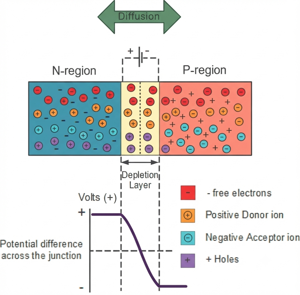
When a PN junction reaches thermal equilibrium, the net diffusion current is balanced by the drift current produced by the internal electric field. The region near the junction contains very few mobile electrons and holes because most of them have recombined, leaving behind fixed ionized atoms.
The depletion layer extends into both the P-type and N-type regions. However, the distances it penetrates into the two sides are not necessarily equal. The width on each side depends on the respective doping concentrations.
Let represent the depletion width extending into the P-type region and represent the width extending into the N-type region. Charge neutrality requires the total magnitude of the negative charge on the P-side to equal the total magnitude of the positive charge on the N-side.
Therefore, for an abrupt PN junction under the depletion approximation:
Where:
- = acceptor concentration in the P-type region
- = donor concentration in the N-type region
- = depletion width within the P-type region
- = depletion width within the N-type region
This relationship shows that the depletion layer extends farther into the more lightly doped side. For example, if the P-side has a higher doping concentration than the N-side, the depletion region penetrates farther into the N-type material.
The total depletion-layer width is:
Thus, the depletion-layer width and its distribution across the two semiconductor regions are determined by their doping concentrations and the junction’s electrical conditions.
Depletion Layer Width and Built-In Electric Potential
When electrons diffuse from the N-type region into the P-type region, they leave behind positively charged donor ions near the junction. Similarly, the movement and recombination of holes on the N-side leave negatively charged acceptor ions in the P-type region. These fixed charges establish an internal electric field across the depletion layer.
The electric field points from the positively charged N-side toward the negatively charged P-side. This field opposes further diffusion of majority charge carriers and creates an energy barrier that carriers must overcome to cross the junction.
The depletion layer extends into both semiconductor regions. Its width depends on the doping concentrations, temperature, and applied voltage. At equilibrium, the internal electric field balances the diffusion tendency, so the net current through the junction is zero.
Built-In Potential Difference Across a PN Junction
The electric field within the depletion region produces a potential difference called the built-in potential or junction potential. It exists across an unbiased PN junction even when no external voltage is applied.
PN Junction Formula:
For an abrupt PN junction at thermal equilibrium, the built-in potential equation across the junction is given by:
Where:
- = Built-in potential difference in volts
- = Thermal voltage, given by (kT/q)
- = Acceptor concentration in the P-type region
- = Donor concentration in the N-type region
- = Intrinsic carrier concentration of the semiconductor
- = Natural logarithm
At approximately 300 K, the thermal voltage is about 25.85 mV for silicon-based calculations.
The equation shows that the built-in potential depends on the doping concentrations and the intrinsic carrier concentration. For a given semiconductor and temperature, increasing the doping concentrations generally increases the built-in potential.
Important: The built-in potential is an internal equilibrium potential, not a voltage that can be measured directly across the terminals of an unbiased diode using an ordinary voltmeter.
Forward and Reverse Biasing of a PN Junction
The electrical behavior of a PN junction changes when an external voltage is applied across it. This process is known as biasing and is classified into two types: forward bias and reverse bias.
In forward bias, the positive terminal of the supply is connected to the P-type region, while the negative terminal is connected to the N-type region. The applied voltage opposes the built-in potential barrier, reducing the electric field across the depletion layer and narrowing its width. As a result, majority charge carriers can cross the junction more easily, allowing a substantial current to flow when the applied voltage is sufficient.
In reverse bias, the positive terminal is connected to the N-type region and the negative terminal to the P-type region. The external voltage reinforces the junction’s electric field, increasing the potential barrier and widening the depletion region. Consequently, the flow of majority carriers is strongly restricted, although a small reverse leakage current may still exist.
Forward Voltage Drop of a PN Junction Diode
The forward voltage drop depends on the semiconductor material, current level, temperature, and diode construction. Typical approximate values for conventional diodes at room temperature are:
- Silicon diode: around 0.6–0.7 V under typical operating conditions.
- Germanium diode: around 0.2–0.3 V, depending on the operating current.
These values are practical forward-voltage approximations, not the built-in potential of an unbiased junction. The built-in potential exists internally at equilibrium, even when no external supply is connected.
Formation and Rectifying Action of a PN Junction Diode
A practical PN junction is generally manufactured by creating adjacent P-type and N-type regions within a single semiconductor crystal. Metal contacts are then added to provide electrical connections to an external circuit.
The resulting device is called a PN junction diode. Its principal characteristic is rectification: it conducts much more readily in forward bias than in reverse bias under normal operating conditions. This property makes PN junction diodes useful in rectifiers, signal-detection circuits, switching applications, and electronic power supplies.
Conclusion
PN junction theory explains how the interaction between P-type and N-type semiconductor regions creates a depletion layer and a built-in potential barrier. By applying forward or reverse bias, the current flow through the junction can be controlled. This principle forms the foundation of PN junction diodes and many semiconductor devices, including rectifiers, transistors, LEDs, and solar cells.
Read Next:
- Diode Voltage Drop: Formula, Values, Chart, Table & Measurement
- Diode Turn-On Voltage: Definition, Values & Examples
- Diode Symbol: Meaning, Types, Circuit Examples
- Diode Terminals: Anode and Cathode Explained
- Diode Polarity: Forward and Reverse Polarity Explained
- What is Reverse Saturation Current?
- Charge Carriers: Definition, Types, Examples, and Working