An Instrumentation Amplifier combines a differential amplifier with cross-coupled input buffer stages to achieve excellent DC accuracy. This configuration provides high precision and makes the circuit well suited for sensor interfaces, measurement systems, and other applications requiring reliable low-level signal amplification.
What is an Instrumentation Amplifier?
An Instrumentation Amplifier (INA) is a precision differential amplifier designed to accurately amplify small voltage differences between two input signals. It generally uses input buffer stages along with a differential amplifier to provide high input impedance, low offset, and high common-mode rejection.
These characteristics make instrumentation amplifiers particularly useful when working with low-level signals from sensors, transducers, strain gauges, thermocouples, and bridge circuits. The amplifier increases the desired differential signal while reducing unwanted signals that are common to both inputs.
To understand how an instrumentation amplifier operates, it is useful to first consider the differential amplifier. A differential amplifier produces an output based on the voltage difference between its two input terminals. Thus, if two input voltages are applied simultaneously, the circuit responds primarily to their difference rather than to their individual values.
The basic relationship can be expressed as:
where is the differential voltage gain, and and are the two input voltages.
The following section explains the basic differential amplifier circuit and its operation, which forms the foundation for understanding the instrumentation amplifier.
Basic Differential Amplifier
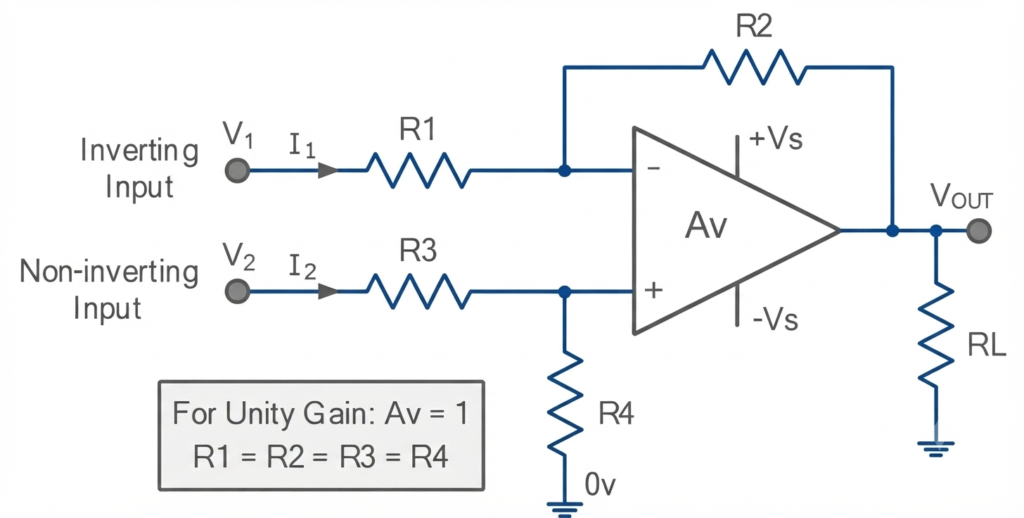
The differential amplifier uses as the input resistor and as the feedback resistor, forming the standard inverting amplifier arrangement. On the non-inverting side, resistors and form a voltage divider that provides the required reference voltage to the op-amp input.
Based on this configuration, the output voltage of the differential amplifier can be determined as follows:
Differential Amplifier Derivation
and,
Output voltage:
For:
that is the ratio:
Thus,
Limitations of the Differential Amplifier
Although a differential amplifier can amplify the voltage difference between two input signals, its input terminals do not necessarily have the same input resistance. The signal applied to sees , whereas the signal at encounters the combined resistance of and .
Therefore, the two inputs are loaded differently because is generally different from . This unequal loading can affect the input signals and reduce the accuracy with which the circuit determines the differential voltage between and .
A differential amplifier is also designed to reject signals that are common to both inputs. These unwanted signals are known as common-mode (CM) signals and may include electrical noise picked up by the input wiring. The ability of the amplifier to suppress these unwanted signals is described by its common-mode rejection ratio (CMRR).
One approach to obtaining good common-mode rejection is to accurately match the resistor ratios:
When these ratios are equal, both input paths have the same voltage gain. However, achieving perfect resistor matching is difficult in practical circuits, so the attainable CMRR is limited by resistor tolerances and matching accuracy.
Another simple arrangement is to select equal resistance values for all four resistors:
With this arrangement, the differential voltage gain becomes unity, and the output is simply the difference between the two input voltages:
This configuration is commonly referred to as a subtractor circuit.
Improving the Basic Subtractor with Input Buffering
The performance of the basic subtractor circuit can be improved considerably by adding a high-input-impedance, unity-gain buffer to each input. This results in a three-op-amp arrangement in which the two input signals are first isolated from the subtractor stage.
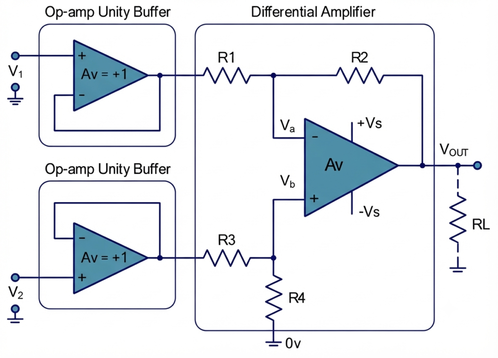
Each buffer operates as a non-inverting voltage follower, providing a high input impedance while maintaining the voltage level of the corresponding input signal. The buffered outputs, designated as and , are then applied to the differential amplifier or subtractor stage formed by the third op-amp.
Because the buffer amplifiers draw very little current from the signal sources, they prevent the subtractor stage from significantly loading the input circuits. This provides the two inputs with closely matched, high-impedance paths and improves the accuracy of differential signal measurement.
In the subtractor stage, and form the familiar inverting op-amp configuration. If and are selected to have equal resistance and the corresponding non-inverting input is connected to ground, the voltage gain of this stage becomes:
Since,
Therfore,
The non-inverting input is connected to the voltage-divider network formed by and . When the two resistors are equal, , the voltage at is given by:
Since,
The voltage is then applied to the non-inverting input of the subtractor stage. The resulting output voltage is:
since,
Therefore,
Then, considering the contribution from the non-inverting input, the overall output voltage can be expressed as:
since,
therfore,
thus,
When all four resistors are selected with the same resistance value, such that , the circuit has a unity differential gain. The output voltage is therefore determined directly by the difference between the two input voltages:
Thus, the circuit operates as a unity-gain subtractor, producing the voltage difference between and .
The key advantage of this buffered subtractor configuration is that the input source impedance has little or no influence on the common-mode signal. The high-input-impedance buffers isolate the signal sources from the differential amplifier and prevent significant loading of the inputs.
The two buffer amplifiers transfer the input signals to the subtractor stage while preserving their voltage levels. Any signal that is common to both inputs appears at both buffer outputs and is subsequently rejected by the differential amplifier. The remaining output is therefore determined primarily by the differential voltage, .
The polarity of the output depends on the relative magnitudes of the two input voltages:
- If , the output voltage is positive.
- If , the output voltage is negative.
- If , the differential output is zero.
The addition of non-inverting buffer stages also makes it possible to adjust the amplifier gain while maintaining the required resistor-ratio matching in the differential stage. By changing the appropriate resistor values, the circuit can provide a controlled differential gain without significantly affecting the high input impedance.
This three-op-amp arrangement forms the basic structure of a precision instrumentation amplifier, which is widely used for amplifying small differential signals from sensors and measurement circuits.
Instrumentation Amplifier Symbol
The instrumentation amplifier symbol resembles the familiar op-amp symbol but includes additional terminals for the gain-setting resistor and the reference voltage . These extra connections indicate the features that distinguish an instrumentation amplifier from a conventional operational amplifier and allow its gain and output reference level to be controlled.
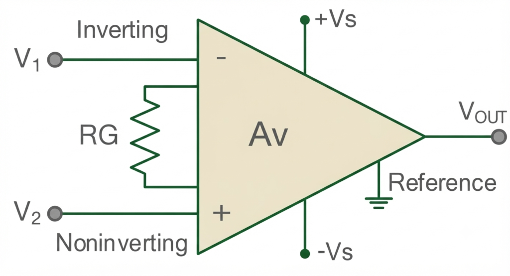
A good understanding of operational amplifiers and instrumentation amplifiers is important in electronics because they serve as fundamental analog building blocks in applications such as signal amplification, sensor interfacing, filtering, measurement, and signal conditioning.
Instrumentation Amplifier Circuit
The buffered three-op-amp subtractor can be further developed by adding voltage gain to the two input buffer stages. This modification produces the conventional three-op-amp instrumentation amplifier and provides a convenient way to control its overall gain.
In this configuration, the gain of the input stage can be adjusted using a single external gain resistor, commonly designated as , which is connected between the two input amplifier stages. This allows the amplifier gain to be changed without disturbing the resistor matching in the differential amplifier stage.
A major advantage of this arrangement is that the differential gain can be set with a single resistor while the precision resistor network in the output stage remains unchanged. This simplifies gain adjustment and helps maintain good common-mode rejection.
The complete instrumentation amplifier uses seven resistors: six resistors associated with the two input amplifier stages and the differential output stage, plus the external gain-setting resistor .
Consider the following instrumentation amplifier circuit:
Instrumentation Amplifier Circuit Duagram
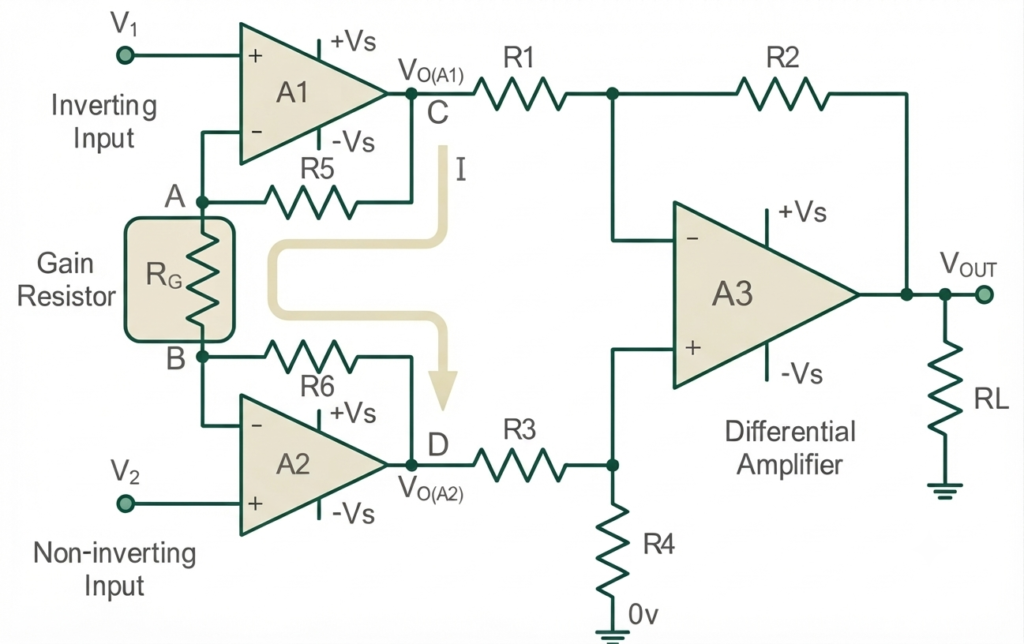
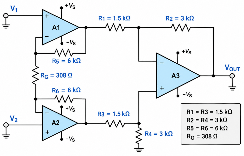
In the three-op-amp instrumentation amplifier, A1 and A2 form the input gain stage, while A3 acts as the differential amplifier that produces the final output. Compared with the basic buffered subtractor, this configuration adds three resistors—, , and the gain-setting resistor —to provide adjustable voltage gain.
The two input op-amps, A1 and A2, operate as non-inverting amplifiers with their outputs cross-coupled through . Because of negative feedback, the voltage at node A follows the input voltage , while the voltage at node B follows . Therefore, the voltage developed across is equal to the difference between the two input voltages:
The voltage difference across produces a current through the resistor. Since the input terminals of ideal op-amps draw essentially no current, the same current must flow through , , and .
Consequently, changing the value of changes the current through the input gain stage and, therefore, changes the differential voltage gain of the instrumentation amplifier. This is the key feature that allows the overall gain to be conveniently adjusted using a single external resistor while maintaining the high input impedance of the two input stages.
Applying Ohm’s law across the voltage difference between nodes and , the current through the gain-setting resistor can be expressed as:
If the two feedback resistors are equal, so that
then the expression simplifies to:
The current through the gain-setting resistor can be expressed in terms of the voltage difference between nodes and :
Since the same current flows through , , and , the two expressions for can be equated:
Rearranging this relationship gives the differential gain of the input stage:
From the previous analysis, the output of the differential amplifier stage can be written in terms of the voltage difference between its two inputs:
Therefore,
Substituting this relationship into the previous gain equation gives:
Hence, the output voltage of the complete instrumentation amplifier can be expressed as:
This equation shows that the overall gain is controlled by the resistor ratios in the differential stage and, importantly, by the single gain-setting resistor . A smaller produces a higher gain, while increasing reduces the gain.
Instrumentation Amplifier Equation

Therefore, the overall differential-mode gain of the instrumentation amplifier can be expressed as:
Instrumentation Amplifier Differential Mode Gain Formula
The differential-mode gain of the instrumentation amplifier is determined by the resistor network in the input gain stage, particularly , , and the gain-setting resistor . If and are selected with equal resistance,
the gain-setting network remains symmetrical, allowing the amplifier gain to be adjusted accurately by changing only .
This is one of the main advantages of the three-op-amp instrumentation amplifier. A single external resistor can be used to set the required differential gain without altering the resistor matching of the differential output stage.
From the differential-mode gain equation,
the required value of the gain-setting resistor can be obtained by rearranging the equation:
For the commonly used unity-gain differential output stage, where , this simplifies to:
This equation can be used to determine the required value of for a desired amplifier gain.
We can extend this analysis by preparing a table that shows the required gain-setting resistor for different values of amplifier gain and feedback resistor , assuming the differential-stage resistors satisfy .
Resistor Values for Different Gain Values
| Total Gain | Bridge Resistances: R5 and R6 | ||||
| Gain | 5 kΩ | 10 kΩ | 25 kΩ | 50 kΩ | 100 kΩ |
| 2 | 2 kΩ | 10 kΩ | 20 kΩ | 50 kΩ | 100 kΩ |
| 5 | 500 Ω | 2.5 kΩ | 5 kΩ | 12.5 kΩ | 25 kΩ |
| 10 | 222 Ω | 1.1 kΩ | 2.2 kΩ | 5.6 kΩ | 11.1 kΩ |
| 20 | 105 Ω | 526 Ω | 1.0 kΩ | 2.6 kΩ | 5.3 kΩ |
| 50 | 41 Ω | 204 Ω | 408 Ω | 1.0 kΩ | 2.0 kΩ |
| 100 | 20 Ω | 101 Ω | 202 Ω | 505 Ω | 1.0 kΩ |
| 200 | 10 Ω | 50 Ω | 100 Ω | 251 Ω | 503 Ω |
| 500 | 4 Ω | 20 Ω | 40 Ω | 100 Ω | 200 Ω |
| 1000 | 2 Ω | 10 Ω | 20 Ω | 50 Ω | 100 Ω |
The table shows that, for a given value of with , the amplifier gain is inversely related to the value of the gain-setting resistor . A smaller produces a higher overall gain, whereas increasing results in a lower gain.
Instrumentation Amplifier Worked Example No. 1
An instrumentation amplifier is used to amplify the 0–40 mV differential signal generated by a resistive strain-gauge bridge. The differential output stage has a voltage gain of 2, while the required overall differential gain of the instrumentation amplifier is 80.
Determine:
- The required value of the gain-setting resistor .
- The maximum output voltage produced by the amplifier.
From the data given, the voltage gain of the differential amplifier is 2. Therefore, if we make the feedback resistor equal to 3 kΩ, the input resistor is calculated as:
Therefore:
As explained previously, the ratios of the differential amplifier resistor pairs and must be matched to provide equal gain from each input leg and thereby improve common-mode rejection.
Therefore:
and,
That is:
and
Also, the gain-determining resistors and , connected across the outputs of the two input buffers, should ideally have the same resistance value to maintain symmetrical operation.
Let us assume a convenient value of 6 kΩ for these resistors. Therefore:
The overall differential gain of the instrumentation amplifier is given by:
Substituting the given values:
Therefore:
A standard resistor value of approximately 308 Ω can therefore be selected to obtain a differential gain close to 80.
The second part of the question is to determine the instrumentation amplifier’s maximum output voltage when the maximum differential input signal from the strain-gauge bridge is 40 mV.
Using:
we get:
Instrumentation Amplifier Worked Example Circuit
Applications of an Instrumentation Amplifier
An Instrumentation Amplifier (INA) is mainly used where small differential signals must be amplified accurately in the presence of noise or unwanted common-mode voltages. Its high input impedance, high common-mode rejection, and adjustable gain make it particularly useful in measurement and signal-conditioning systems.
Common applications include:
- Strain Gauge Measurements: Used with Wheatstone bridge circuits to amplify the small voltage changes produced by strain gauges.
- Temperature Measurement: Interfaces with thermocouples, RTDs, and other temperature sensors that generate low-level signals.
- Pressure and Load Sensors: Amplifies the differential output of pressure transducers, load cells, and force sensors.
- Biomedical Instrumentation: Used to amplify small electrical signals from sensors and electrodes in equipment such as ECG and EEG systems.
- Data Acquisition Systems: Provides accurate signal conditioning before low-level sensor signals are fed to an ADC.
- Industrial Process Measurement: Used with transmitters and sensors for measuring pressure, flow, level, temperature, and other process variables.
- Bridge Circuit Applications: Amplifies differential outputs from resistive and capacitive bridge networks while rejecting common-mode interference.
- Current Sensing: Measures the small voltage developed across a shunt resistor while rejecting the common-mode voltage present on the monitored line.
- Weighing Systems: Used with load cells to amplify their very small differential output signals before further processing.
- Audio and Signal Conditioning: Can be used where a differential low-level signal requires amplification with good rejection of unwanted common-mode noise.
Overall, the instrumentation amplifier is especially valuable in precision measurement and sensor-interface applications where signal accuracy and noise rejection are important.
Conclusion
An Instrumentation Amplifier is a precision differential amplifier designed to amplify small voltage differences while providing high input impedance and excellent common-mode signal rejection. Its three-op-amp configuration uses two input buffer amplifiers to isolate the signal sources and a differential amplifier to produce the final output.
A major advantage of this configuration is its single-resistor gain adjustment. The overall differential gain can be controlled by changing the gain-setting resistor , while the matched resistor network in the differential stage helps maintain good common-mode rejection.
The differential-mode gain is given by:
Thus, reducing increases the amplifier gain, whereas increasing reduces it. Because of its accurate gain control, high input impedance, and ability to amplify low-level differential signals, the instrumentation amplifier is widely used in sensor interfaces, strain-gauge circuits, bridge measurements, data-acquisition systems, and industrial measurement applications.
Read Next:
- Inverting vs Non-Inverting Amplifier: Differences, Gain, and Applications
- Inverting Operational Amplifier: Circuit, Working, and Gain Formula
- Op-Amp Building Blocks: Basic Circuits and Applications
- Operational Amplifier (Op-Amp): Basics, Types, Working & Applications
- Non-inverting Operational Amplifier: Circuit, Gain & Formula
- Summing Amplifier: Circuit, Gain Formula, Derivation & Applications
- Differential Amplifier: Circuit, Types, Formula & Applications
- Op-Amp Integrator Amplifier: Formula, Working & Applications
- Op-Amp Differentiator Amplifier: Circuit, Working, Formula & Applications
- Op-Amp Multivibrator: Working, Circuit, Types & Applications
- Op-Amp Comparator: Circuit, Working, Formula, Hysteresis & Applications
- Op-Amp Monostable Multivibrator: Circuit, Working, Formula & Timing
- Passive Averager: Circuit, Equation & Op-Amp Averager
- Transimpedance Amplifier: Circuit, Formula & Applications
- CMRR of Op-Amp: Formula, Definition, Measurement, Applications
- Slew Rate: Definition, Formula, Unit, Calculation, Measurement & Applications