A PN-junction diode is created by joining p-type and n-type semiconductor materials. This junction develops a built-in potential barrier that regulates the movement of charge carriers across the interface.
What Is a PN Junction Diode?
A PN junction diode is a two-terminal semiconductor device formed by joining p-type and n-type semiconductor regions. At the interface between these regions, electrons and holes recombine, creating a depletion region that contains very few mobile charge carriers. This region establishes an internal electric field and a built-in potential barrier that opposes further diffusion of charge carriers.
When no external voltage is applied, the diode reaches thermal equilibrium. Although electrons and holes continue to move microscopically, the opposing effects of diffusion and the electric field balance each other, resulting in zero net current. The semiconductor as a whole remains electrically neutral, even though fixed positive and negative ions are present within the depletion region.
When a battery is connected across the diode, the applied voltage changes the potential barrier and the width of the depletion region. Under forward bias, the barrier decreases, allowing a substantial current to flow through the junction. Under reverse bias, the barrier increases, so only a very small leakage current normally flows.
This difference in current flow makes the PN junction diode useful for controlling the direction of current in an electrical circuit. It is widely used in rectifiers, switching circuits, signal detection, and voltage protection applications.
Formation of a PN Junction
A PN junction is created by forming p-type and n-type regions within a semiconductor crystal, usually silicon or germanium. The p-type region contains holes as the majority charge carriers, whereas the n-type region contains electrons as the majority carriers.
When these two regions are brought together, a concentration difference causes holes to move from the p-side to the n-side and electrons to move from the n-side to the p-side. This movement of charge carriers is called diffusion, and the resulting current is known as diffusion current.
As electrons cross the junction and recombine with holes, they leave behind positively charged donor ions on the n-side. Similarly, holes moving away from the p-side leave negatively charged acceptor ions. These immobile ions create a region around the junction that is depleted of mobile charge carriers. This region is called the depletion region.
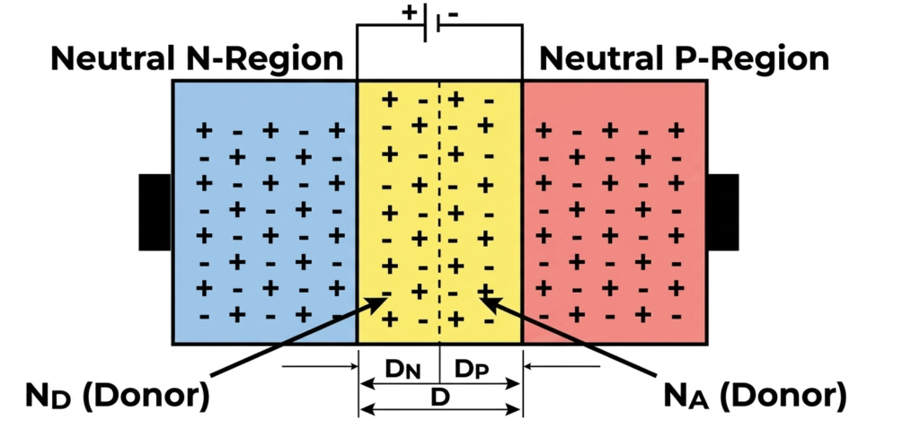
The charged ions establish an electric field directed from the positively charged donor ions on the n-side toward the negatively charged acceptor ions on the p-side. This field opposes further diffusion and produces a drift current in the direction opposite to the diffusion current.
At thermal equilibrium, the drift current and diffusion current balance each other. Consequently, the net current through the unbiased PN junction is zero, and a built-in potential barrier is established across the depletion region.
P-N Junction Formula
The P-N junction formula is used to calculate the built-in potential (also called the contact potential) developed across a semiconductor junction under thermal equilibrium and zero external bias.
The built-in potential is expressed as:
Where:
- = Built-in potential of the P-N junction (V)
- = Thermal voltage, approximately 26 mV at room temperature (300 K)
- = Donor concentration in the n-type region
- = Acceptor concentration in the p-type region
- = Intrinsic carrier concentration of the semiconductor
The logarithm used in this equation is the natural logarithm, denoted by . The built-in potential depends on the doping concentrations and the intrinsic carrier concentration of the semiconductor.
Biasing Conditions of a PN Junction Diode
A PN junction diode consists of two semiconductor regions:
- P-type region
- N-type region
Depending on the applied voltage, a PN junction diode can operate under three biasing conditions:
- Zero bias: No external voltage is applied across the PN junction diode.
- Forward bias: The P-type region is connected to the positive terminal of the voltage source, while the N-type region is connected to the negative terminal.
- Reverse bias: The P-type region is connected to the negative terminal of the voltage source, while the N-type region is connected to the positive terminal.
Forward-Biased PN Junction Diode
A PN junction diode is forward-biased when the p-type region is connected to the positive terminal of a battery and the n-type region is connected to the negative terminal. In this condition, the applied electric field acts opposite to the built-in electric field across the junction, reducing the potential barrier.
Unlike a fixed resistor, a diode has a nonlinear current-voltage (I-V) characteristic. Its current increases rapidly with the applied forward voltage and cannot be described using Ohm’s law with a constant resistance.
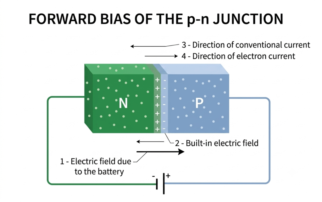
When forward bias is applied, the opposing electric fields reduce the effective potential barrier and narrow the depletion region. This allows majority charge carriers to cross the junction more easily, resulting in an increase in current.
For a silicon diode, the forward voltage drop is commonly around 0.6–0.7 V under typical operating conditions, although the actual value depends on the current, temperature, and diode characteristics. As the forward voltage increases, the diode conducts more current and exhibits relatively low dynamic resistance. However, the depletion region does not become completely resistance-free, so an appropriate current-limiting arrangement may be required to protect the diode.
Reverse-Biased PN Junction
A PN junction diode is reverse-biased when the p-type region is connected to the negative terminal of a battery and the n-type region is connected to the positive terminal. Under this condition, the applied electric field acts in the same direction as the built-in electric field across the junction.
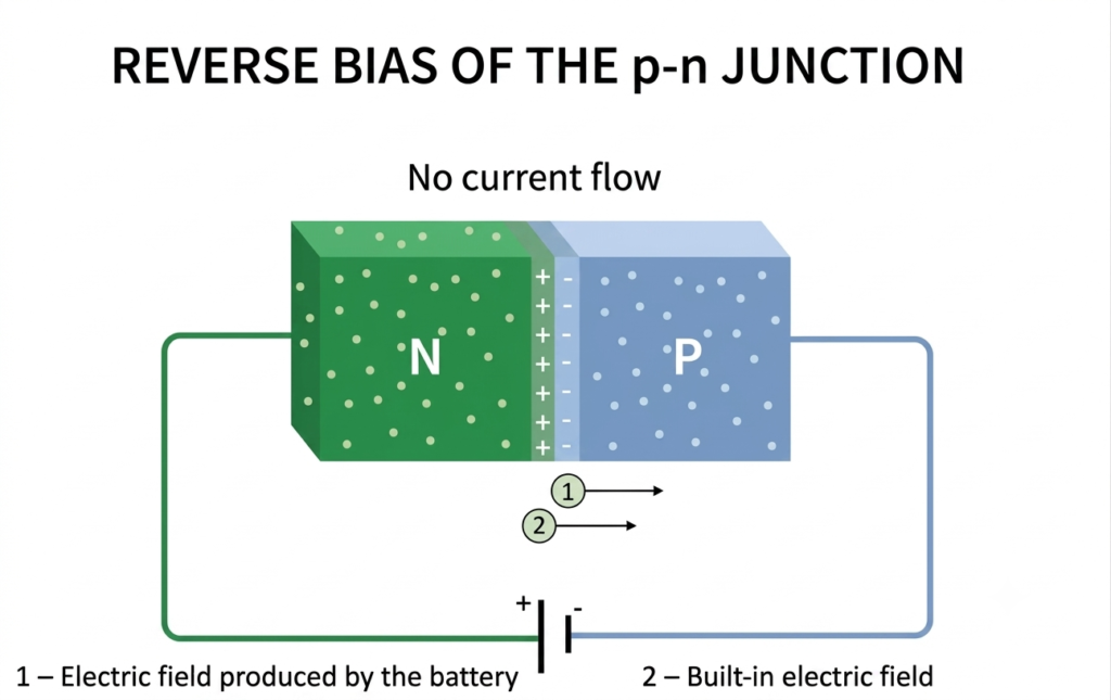
The two electric fields reinforce each other, increasing the potential barrier and widening the depletion region. This makes it more difficult for majority charge carriers to cross the junction, causing the diode to exhibit very high resistance.
Reverse bias does not completely prevent current flow. A small reverse leakage current continues to flow due to minority charge carriers, but it is generally negligible under normal operating conditions. As the applied reverse voltage increases, the depletion region becomes wider and the diode continues to block the flow of current.
If the reverse voltage reaches the diode’s breakdown voltage, the reverse current can increase sharply. A current-limiting arrangement is required to prevent damage unless the diode is specifically designed to operate in the breakdown region.
In contrast, forward bias reduces the potential barrier and narrows the depletion region, allowing current to flow more easily. This difference in the diode’s response to forward and reverse voltages produces its rectifying characteristic.
Rectification is the conversion of alternating current (AC) into unidirectional current. A PN junction diode performs this function by conducting readily under forward bias while restricting current under reverse bias, as illustrated by its static current-voltage (I-V) characteristics.
PN Junction Diode Symbol and Static I-V Characteristics
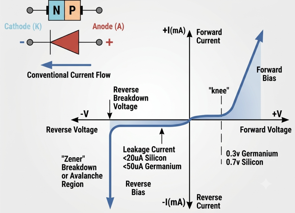
The voltage applied across a PN junction determines whether the potential barrier increases or decreases. A voltage that raises the barrier is associated with reverse bias, whereas a voltage that lowers the barrier is associated with forward bias.
A standard PN junction diode operates under three biasing conditions:
- Zero Bias: No external voltage is applied across the PN junction.
- Reverse Bias: The negative terminal of the supply is connected to the p-type region, and the positive terminal is connected to the n-type region. This increases the potential barrier and widens the depletion region.
- Forward Bias: The positive terminal of the supply is connected to the p-type region, and the negative terminal is connected to the n-type region. This reduces the potential barrier and narrows the depletion region.
Zero-Biased PN Junction Diode
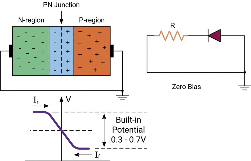
A PN junction diode is said to be zero-biased, or unbiased, when no external voltage is applied across its terminals ((V=0)). Even in this condition, charge carriers move across the junction because the p-type region contains a high concentration of holes, while the n-type region contains a high concentration of electrons.
Due to this concentration difference, electrons diffuse from the n-side to the p-side, while holes diffuse from the p-side to the n-side. When these carriers recombine near the junction, they leave behind fixed charged ions, forming a depletion region and establishing a built-in potential barrier.
At the same time, the electric field within the depletion region causes charge carriers to drift in the direction opposite to diffusion. The diffusion current and drift current balance each other at thermal equilibrium, resulting in zero net current through the unbiased diode.
Although individual charge carriers continue to move, there is no continuous net current through the junction. The built-in potential barrier prevents further net diffusion of majority carriers under equilibrium conditions.
For a typical silicon diode, the built-in potential is often approximately 0.6–0.7 V at room temperature, while for a germanium diode, it is commonly around 0.2–0.3 V. These values depend on factors such as doping concentration and temperature. The built-in potential is an internal junction potential, not an externally measurable terminal voltage across an unbiased diode.
The potential barrier that develops across the PN junction opposes the further diffusion of majority charge carriers. However, the electric field within the depletion region allows minority charge carriers, such as electrons in the p-type region and holes in the n-type region, to drift across the junction.
Eventually, the diffusion current and drift current become equal in magnitude and flow in opposite directions. As a result, the net current through the junction becomes zero. This balanced condition is known as dynamic equilibrium.
At equilibrium, a stable depletion region is maintained near the junction. It contains very few mobile charge carriers because most electrons and holes in this region have recombined, leaving behind fixed positive donor ions and negative acceptor ions.
Minority charge carriers are continuously generated by thermal energy within the semiconductor. An increase in temperature generally increases the generation of these carriers, resulting in a higher reverse leakage current when the diode is connected in a circuit. However, under thermal equilibrium with no external voltage applied, the diffusion and drift currents continue to balance each other, so the net current remains zero.
Reverse Biasing a PN Junction Diode
A reverse-biased PN junction diode is formed by connecting the positive terminal of a voltage source to the n-type region and the negative terminal to the p-type region.
Under this condition, electrons in the n-type region are attracted toward the positive terminal, while holes in the p-type region move toward the negative terminal. This movement of majority charge carriers away from the junction widens the depletion region.
As the depletion region expands, the potential barrier across the junction increases, making it more difficult for majority carriers to cross. Consequently, the diode offers very high resistance and behaves approximately like an open switch, allowing only a negligible current to flow under normal reverse-bias conditions.
Increase in the Depletion Layer Due to Reverse Bias
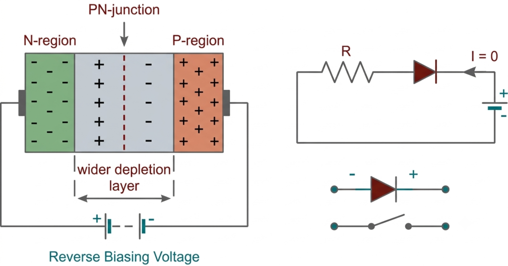
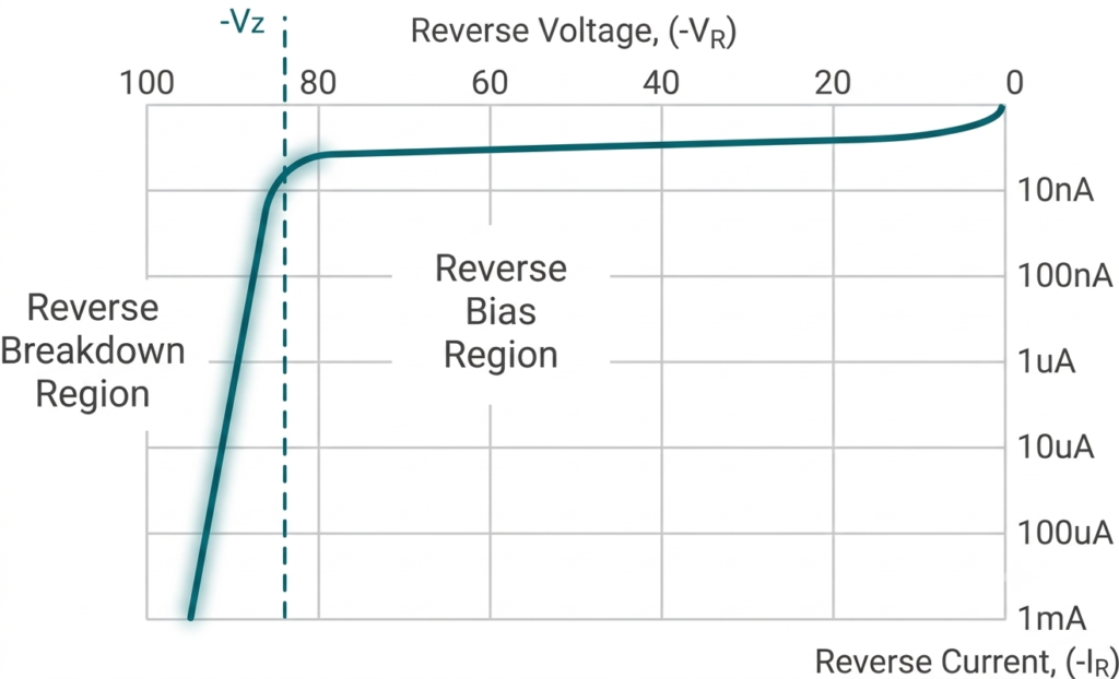
When the reverse-bias voltage increases, the depletion region generally becomes wider, further restricting the movement of majority carriers. However, a small reverse leakage current continues to flow because of minority charge carriers. In many small-signal diodes, this current is very low, although its magnitude depends on the diode type, temperature, and applied voltage.
If the reverse voltage reaches a sufficiently high value, the diode enters the breakdown region. Depending on the diode structure and operating conditions, breakdown occurs through the Zener effect or the avalanche effect. During avalanche breakdown, charge carriers gain enough energy from the electric field to generate additional electron-hole pairs through collisions, causing the reverse current to rise sharply.
Breakdown does not necessarily damage a diode. A diode designed for breakdown operation can function safely when the current is properly limited. However, an ordinary diode may overheat and fail if excessive reverse current flows without adequate protection. The breakdown voltage is represented on the reverse side of the diode’s static current-voltage (I-V) characteristic by a sharp increase in reverse current. For example, a particular diode might have a breakdown voltage of approximately −80 V, depending on its specifications.
Reverse Characteristics Curve of a PN Junction Diode
The avalanche breakdown effect can be useful in electronic circuits that require voltage regulation. A Zener diode is a specially designed, heavily doped PN junction diode that can operate repeatedly in its reverse-breakdown region without damage, provided the current and power dissipation remain within its rated limits.
When forward-biased, a Zener diode behaves like a conventional silicon diode. It conducts current when the anode is sufficiently positive relative to the cathode, typically producing a forward voltage drop of around 0.7 V under normal operating conditions.
Under reverse bias, the Zener diode initially permits only a small leakage current. When the reverse voltage reaches its specified breakdown voltage, , the reverse current increases significantly. The voltage across the diode remains approximately constant over its intended operating range, making it useful for maintaining a stable output voltage.
A series current-limiting resistor, commonly represented by , is generally used to restrict the reverse current to a safe value and protect the diode from excessive power dissipation. This property makes Zener diodes suitable for voltage stabilization, reference-voltage generation, and overvoltage protection. The 1N4733A is an example of a Zener diode with a nominal breakdown voltage of 5.1 V.
Forward Biasing a PN Junction Diode
A forward-biased PN junction diode is formed by connecting the positive terminal of a voltage source to the p-type region and the negative terminal to the n-type region. The applied electric field opposes the built-in electric field at the junction, reducing the potential barrier and narrowing the depletion region.
As the forward voltage increases, majority charge carriers gain sufficient energy to cross the junction more easily. Electrons from the n-type region move toward the p-side, while holes from the p-type region move toward the n-side. These carriers cross the junction and contribute to the forward current.
For a typical silicon diode, the forward voltage drop is commonly around 0.6–0.7 V, whereas a germanium diode often has a forward voltage drop of approximately 0.2–0.3 V. These values are approximate and vary with the diode’s operating current, temperature, and construction. The applied voltage does not need to exceed the built-in potential barrier as a strict threshold before current can flow.
Once the diode conducts significantly, a relatively small increase in forward voltage can produce a large increase in current. This behavior is represented by the diode’s current-voltage (I-V) characteristic curve, where the forward current rises rapidly around the knee region. An appropriate current-limiting resistor is generally needed to prevent excessive current from damaging the diode.
Forward Characteristics Curve of a PN Junction Diode
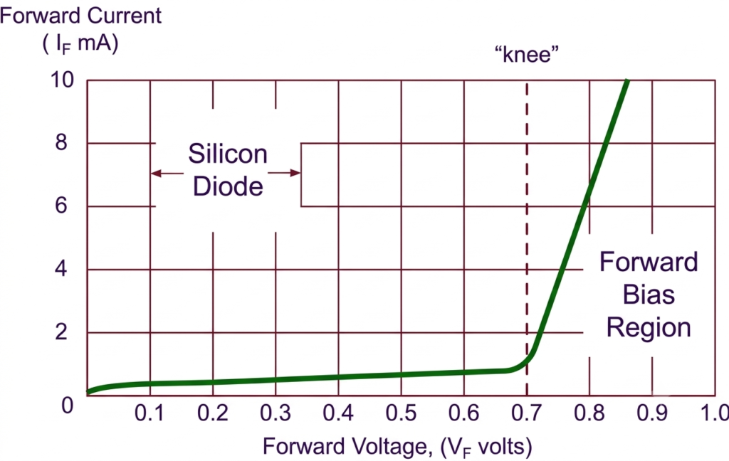
When the forward voltage applied to a PN junction diode increases, the potential barrier decreases and the depletion region becomes narrower. As the diode enters its conducting region, the current rises rapidly, and the diode offers relatively low dynamic resistance.
For a typical silicon diode, substantial forward conduction commonly occurs around 0.6–0.7 V, although the actual voltage depends on the diode’s characteristics, current, and temperature.
The point on the static current-voltage (I-V) characteristic curve where the forward current begins to increase sharply is known as the knee point or cut-in voltage. Beyond this region, a small increase in forward voltage can produce a significant increase in current.
Reduction in the Depletion Layer Due to Forward Bias
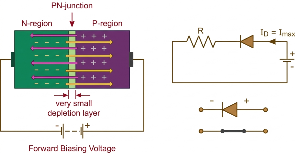
When a PN junction diode is forward-biased, the depletion region becomes narrower, reducing the resistance of the junction and allowing current to increase significantly with a small rise in the applied voltage. The forward voltage drop is typically around 0.3 V for a germanium diode and 0.7 V for a silicon diode under common operating conditions, although the actual values depend on current and temperature.
Beyond the knee point, the diode conducts substantial current and behaves approximately like a closed switch. However, it does not become a perfect short circuit, and the current is not unlimited. Therefore, a series resistor or suitable load impedance is required to keep the forward current within the diode’s maximum rated limit.
If the current exceeds the specified rating, the diode may dissipate excessive power as heat. This can cause overheating, damage to the semiconductor junction, and eventual device failure. Proper current limiting is essential for safe and reliable diode operation.
Applications of a P-N Junction Diode
A P-N junction diode is widely used in electronic circuits because of its ability to conduct current primarily in one direction. Some of its common applications are listed below:
- Rectification: A P-N junction diode is used in rectifier circuits to convert alternating current (AC) into direct current (DC).
- Voltage regulation: A Zener diode, a special type of P-N junction diode, is used to maintain a nearly constant voltage across a load.
- Electronic switching: A diode can act as a switch in electronic circuits by controlling current flow under forward- and reverse-bias conditions.
- Light detection: A photodiode typically operates under reverse bias to detect incident light and convert it into an electrical current.
- Light emission: A light-emitting diode (LED) produces light when it is forward-biased and current flows through its junction.
For more information, read our detailed article on Applications of PN junction diode
Conclusion
A PN junction diode is a fundamental semiconductor device formed by joining p-type and n-type materials. The junction develops a depletion region and a built-in potential barrier that control the movement of charge carriers. Under forward bias, the barrier decreases and current flows readily, whereas reverse bias widens the depletion region and restricts current flow until breakdown occurs. Understanding the formation, biasing conditions, current-voltage characteristics, and built-in potential of a PN junction diode helps explain its important role in rectifiers, electronic switching, voltage regulation, and other semiconductor applications.
Read Next: